NCP308, NCV308
www.onsemi.com
7
DETAILED DESCRIPTION
The NCP308 microprocessor supervisory product family
is designed to assert a RESET
signal when either the SENSE
pin voltage drops below V
IT
or the Manual Reset input (MR)
is driven low. The RESET
output remains asserted for a
programmable delay time after both MR
and SENSE
voltages return above the respective thresholds. A broad
range of voltage threshold and reset delay time options are
available, allowing NCP308 series to be used in a wide range
of applications.
Reset threshold voltages can be factory−set from 0.82 V
to 3.3 V or from 4.4 V to 5.0 V, while the NCP308XXADJ
can be used for any voltage above 0.405 V using an external
resistor divider.
Flexible delay time can be easily got with CT pin
according to Table 5:
Table 5. DELAY TIME SETTING TABLE
CT pin Configuration Delay Time (tD)
CT = VDD 300 ms (fixed)
CT = Open 20 ms (fixed)
Connecting a capacitor be-
tween pin CT and GND
(Capacitor CT value >
100 pF)
1.25 ms ~ 10 s, depends on
capacitor value (Refer to the
Setting Reset Delay Time
Section)
Output
The RESET output is typically connected to the RESET
control pin of a microprocessor. For Open−Drain output
versions, a pull−up resistor must be used to hold this line
high when RESET
is not asserted. The RESET output is
active once V
DD
is over V
DD
(min), this voltage is much
lower than most microprocessors’ functional voltage range.
RESET
remains high as long as SENSE is above its
threshold (V
IT
) and the Manual Reset input (MR) is logic
high. If either SENSE falls below V
IT
or MR is driven low,
RESET
is asserted.
Once MR
is again logic high and SENSE is above (V
IT
+
V
HYS
), the RESET pin goes to a high impedance state after
delay time (tD). The open−drain structure of RESET
is
capable to allow the reset signal for the microprocessor to
have a voltage higher than V
DD
(up to 5.5 V). The pull−up
resistor should be no smaller than 10 kW as a result of the
finite impedance of the RESET
line.
SENSE Input
The SENSE input should be connected to the monitored
voltage directly. If the voltage on this pin drops below V
IT
,
then RESET
is asserted. The comparator has a built−in
hysteresis to prevent erratic reset operation. It is good
practice to put a 1 nF to 10 nF bypass capacitor on the
SENSE input to reduce its sensitivity to transients and layout
parasitic.
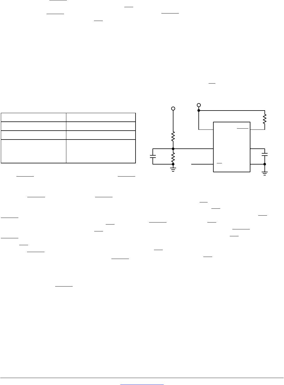
The NCP308XXADJ can be used to monitor any voltage
rail down to 0.405 V by the circuit shown in Figure 12. The
new V
IT
’ can be derived from resistor divider network of R1
and R2 by:
V
IT
Ȁ+
ǒ
R1
R2
) 1
Ǔ
V
IT
(eq. 1)
VIN
VDD
(Optional)
Rpullup
SENSE CT
GND
VDD
CT
R1
R2
1 nF
(Optional)
NCP308XXADJ
Figure 12. Using NCP308XXADJ to Monitor a
User−Defined Threshold Voltage
MR
RESET
MR
Manual Reset Input (MR)
The Manual Reset input (MR) allows a processor or other
logic circuits to initiate a reset. A logic low on MR
causes
RESET
to assert. After MR returns to a logic high and
SENSE is above its reset threshold, RESET
is de−asserted
after the delay time set by CT pin. MR
is internally tied to
V
DD
by a 90 kW resistor so this pin can be left unconnected
if MR
will not be used.
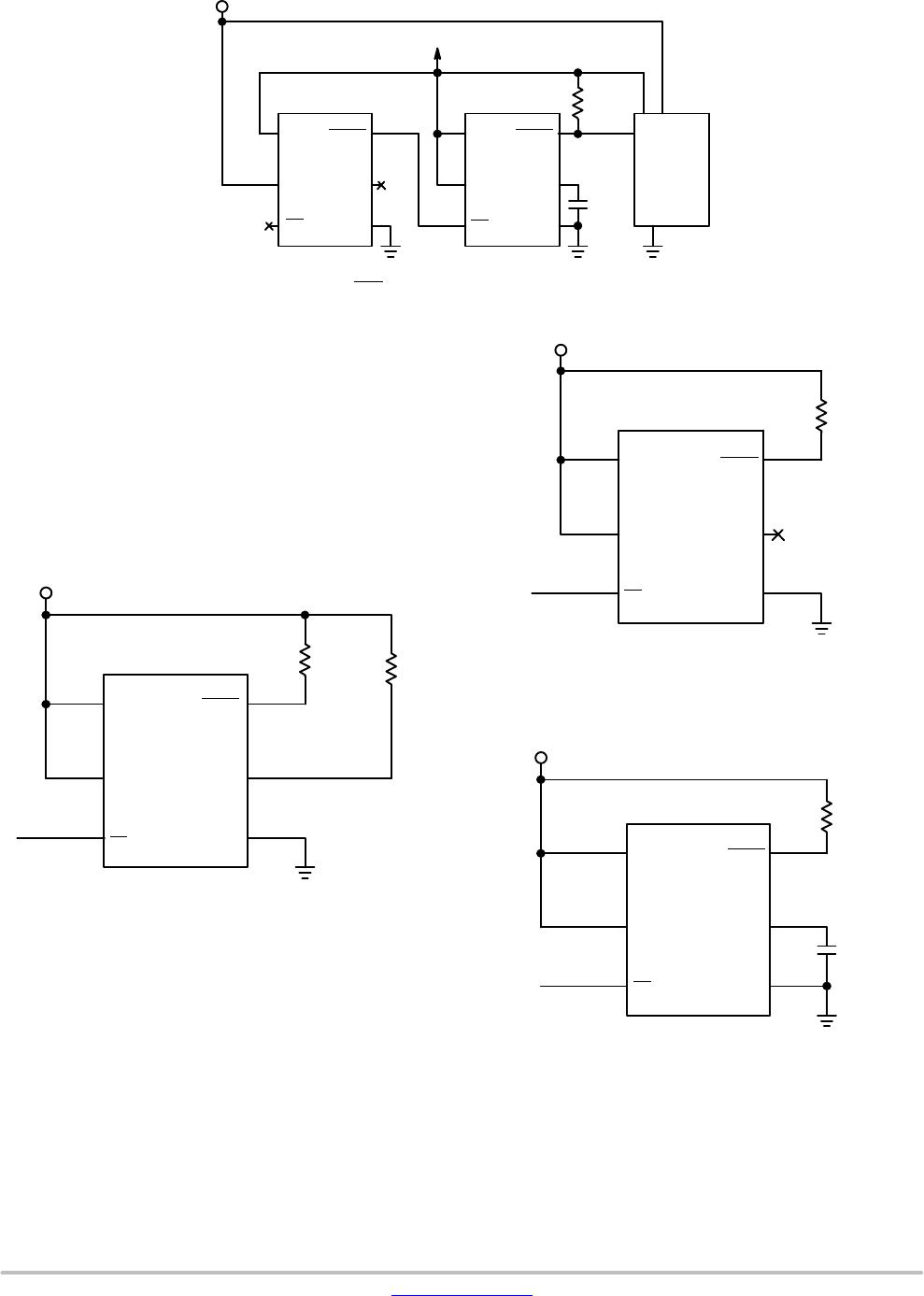
Figure 13 shows how MR
can be used to monitor multiple
system voltages (e.g. I/O supply voltage of some
DSP/processors should be setup before core voltage, and
DSP/processor can only start after both I/O and core
voltages setup).