2
COMMERCIAL AND INDUSTRIAL TEMPERATURE RANGES
IDT2309NZ
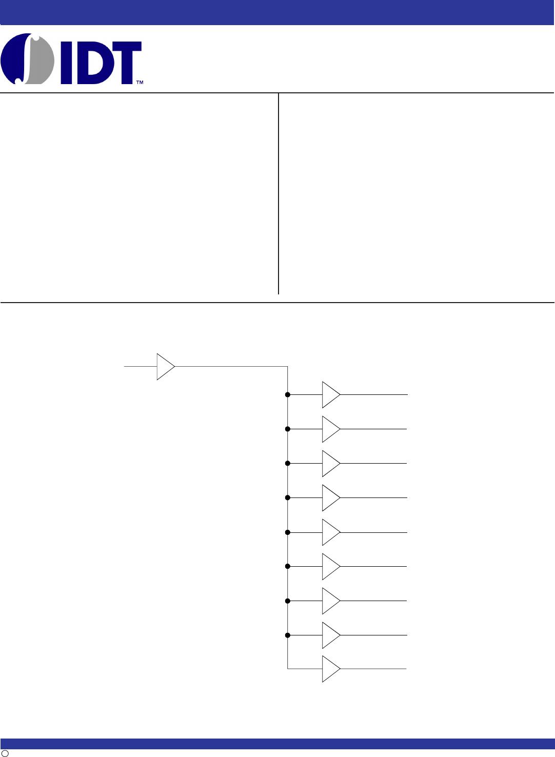
NINE OUTPUT 3.3V CLOCK BUFFER
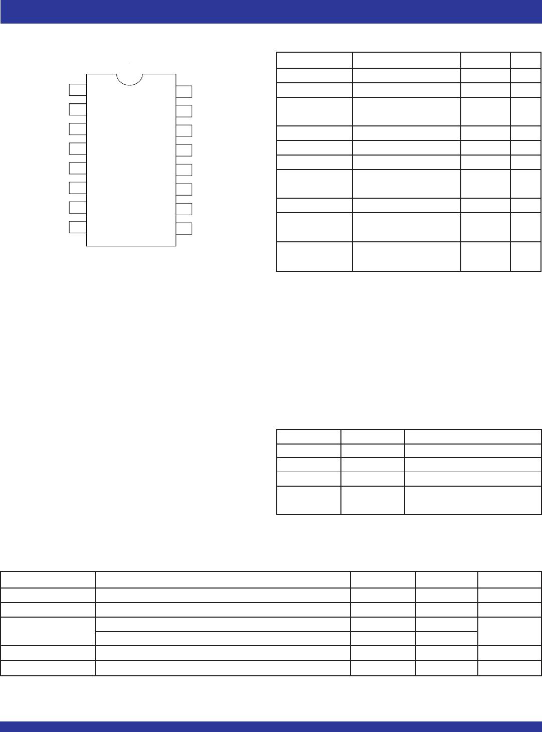
PIN CONFIGURATION
SOIC/ TSSOP
TOP VIEW
BUF_IN
OUTPUT1
VDD
2
3
4
5
6
7
8
9
10
11
12
13
14
15
161
OUTPUT2
GND
OUTPUT3
OUTPUT9
OUTPUT8
GND
GND
VDD
VDD
OUTPUT4
OUTPUT5
OUTPUT6
OUTPUT7
PIN DESCRIPTION
Pin Name Pin Number Functional Description
VDD 4, 8, 13 3.3V Digital Voltage Supply
GND 5, 9, 12 Ground
BUF_IN 1 Input clock
OUTPUT[1:9] 2, 3, 6, 7, 10 Outputs
11, 14, 15, 16
Symbol Parameter Min. Max. Unit
VDD Supply Voltage 3 3.6 V
TA Operating Temperature (Ambient Temperature) 0 70 ° C
CL Load Capacitance, FOUT < 100MHz — 30 pF
Load Capacitance 100MHz < FOUT < 133.33MHz — 15
CIN Input Capacitance — 7 pF
BUF_IN, SDRAM[1:9] Operating Frequency DC 133.33 MHz
OPERATING CONDITIONS - COMMERCIAL
Symbol Rating Max. Unit
VDD Supply Voltage Range –0.5 to +4.6 V
VI
(2)
Input Voltage Range (REF) –0.5 to +5.5 V
VI Input Voltage Range –0.5 to V
(except REF) VDD+0.5
IIK (VI < 0) Input Clamp Current –50 mA
IO (VO = 0 to VDD) Continuous Output Current ±50 mA
VDD or GND Continuous Current ±100 mA
TA = 55°C Maximum Power Dissipation 0.7 W
(in still air)
(3)
TSTG Storage Temperature Range –65 to +150 °C
Operating Commercial Temperature 0 to +70 °C
Temperature Range
Operating Industrial Temperature -40 to +85 °C
Temperature Range
NOTES:
1. Stresses greater than those listed under ABSOLUTE MAXIMUM RATINGS may cause
permanent damage to the device. This is a stress rating only and functional operation
of the device at these or any other conditions above those indicated in the operational
sections of this specification is not implied. Exposure to absolute maximum rating
conditions for extended periods may affect reliability.
2. The input and output negative-voltage ratings may be exceeded if the input and output
clamp-current ratings are observed.
3. The maximum package power dissipation is calculated using a junction temperature
of 150°C and a board trace length of 750 mils.
ABSOLUTE MAXIMUM RATINGS
(1)