NTVB200SA-L

© Semiconductor Components Industries, LLC, 2010
October, 2010 Rev. 0
1 Publication Order Number:
NTVB058NS/D
NTVB Series
Thyristor Surge Protectors
High Voltage Bidirectional
NTVB Series Thyristor Surge Protector Devices (TSPD) protect
telecommunication circuits such as central office, access, and
customer premises equipment from overvoltage conditions. These are
bidirectional devices so they are able to have functionality of 2 devices
in one package, saving valuable space on board layout.
These devices will act as a crowbar when overvoltage occurs and will
divert the energy away from circuit or device that is being protected.
Use of the NTVB Series in equipment will help meet various
regulatory requirements including: GR1089CORE, IEC
6100045, ITU K.20/21/45, IEC 60950, TIA968A, FCC Part 68,
EN 60950, UL 1950.
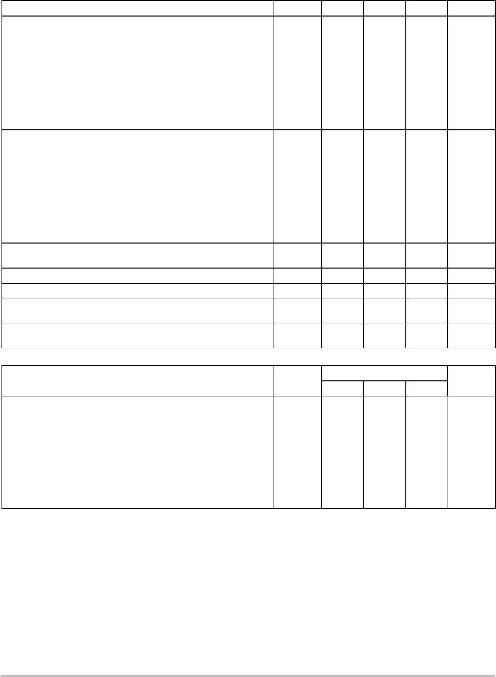
ELECTRICAL PARAMETERS
Device
V
DRM
V
(BO)
V
T
I
DRM
I
(BO)
I
T
I
H
V V V
mA
mA A mA
NTVB058NSxL 58 77 4 5 800 2.2 150
NTVB065NSxL 65 88 4 5 800 2.2 150
NTVB090NSxL 90 130 4 5 800 2.2 150
NTVB170SxL 170 265 4 5 800 2.2 150
NTVB170NSxL 170 220 4 5 800 2.2 150
NTVB180SxL 170 240 4 5 800 2.2 150
NTVB200SxL 200 320 4 5 800 2.2 150
NTVB220NSxL 220 300 4 5 800 2.2 150
NTVB270SxL 270 365 4 5 800 2.2 150
NTVB275NSxL 275 350 4 5 800 2.2 150
NTVB300SxL 300 400 4 5 800 2.2 150
SURGE DATA RATINGS
Specification
Waveform x = series ratings
Unit
Voltage
ms
Current
ms
A B C
GR1089CORE 2x10 2x10 150 250 500
A(pk)
TIA968A 10x160 10x160 90 150 200
GR1089CORE 10x360 10x360 75 125 175
TIA968A 10x560 10x560 50 100 150
ITUT K.20/21 10x700 5x310 75 100 200
GR1089CORE 10x1000 10x1000 50 80 100
* Recognized Components
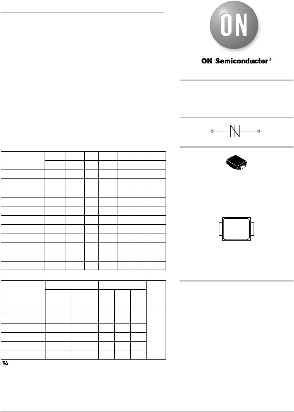
BIDIRECTIONAL SURFACE
MOUNT THYRISTOR
64 350 VOLTS
MT1 MT2
SMB
JEDEC DO214AA
CASE 403C
XXXX = Specific Device Code
Y = Year
WW = Work Week
G = PbFree Package
(Note: Microdot may be in either location)
MARKING DIAGRAM
AYWW
XXXXG
G
http://onsemi.com
See detailed ordering and shipping information on page 4 of
this data sheet.
ORDERING INFORMATION
NTVB Series
http://onsemi.com
2
ELECTRICAL CHARACTERISTICS (T
A
= 25°C unless otherwise noted)
Characteristics (Notes 1, 2, 3)
Symbol Min Typ Max Unit
Breakover Voltage (Both Polarities)
NTVB058NSxL
NTVB065NSxL
NTVB090NSxL
NTVB170SxL
NTVB170NSxL
NTVB180SxL
NTVB200SxL
NTVB220NSxL
NTVB270SxL
NTVB275NSxL
NTVB300SxL
V
(BO)
77
88
130
265
220
240
320
300
365
350
400
V
OffState Voltage (Both Polarities)
NTVB058NSxL
NTVB065NSxL
NTVB090NSxL
NTVB170SxL
NTVB170NSxL
NTVB180SxL
NTVB200SxL
NTVB220NSxL
NTVB270SxL
NTVB275NSxL
NTVB300SxL
V
DRM
58
65
90
170
170
170
200
220
270
275
300
V
Off State Current ( V
D1
= 50 V ) Both Polarities
( V
D2
= V
DRM
) Both Polarities
I
DRM1
I
DRM2
2.0
5.0
mA
mA
Holding Current (Both Polarities) (Note 3) V
S
= 500 V; I
T
= 2.2 A I
H
150 250 mA
OnState Voltage I
T
= 1.0 A(pk) (PW = 300 mSec, DC = 2%)
V
T
4.0 V
Maximum NonRepetitive Rate of Change of OnState Current (Note 1)
(Haefely test method, 1.0 pk < 100 A)
di/dt 500
A/mSec
Critical Rate of Rise of OffState Voltage
(Linear Waveform, V
D
= 0.8 V
DRM
, T
J
= 25°C)
dv/dt 5.0
kV/mSec
CAPACITANCE
Characteristics Symbol
Typ
Unit
A B C
(f=1.0 MHz, 1.0 V
rms
, 2 Vdc bias)
NTVB058NSxL
NTVB065NSxL
NTVB090NSxL
NTVB170SxL
NTVB170NSxL
NTVB180SxL
NTVB200SxL
NTVB220NSxL
NTVB270SxL
NTVB275NSxL
NTVB300SxL
C
o
84
79
58
39
39
37
36
33
31
28
28
129
123
95
150
59
59
56
52
47
44
44
222
198
154
195
99
97
110
81
76
97
71
pF
1. Electrical parameters are based on pulsed test methods.
2. Measured under pulsed conditions to reduce heating
3. Allow cooling before testing second polarity.
NTVB Series
http://onsemi.com
3
SURGE RATINGS
Characteristics
Symbol A B C Unit
Nominal Pulse
Surge Short Circuit Current Non – Repetitive
Double Exponential Decay Waveform (Notes 4, 5 and 6)
2 x 10 mSec
10 x 160 mSec
10 x 360 mSec
10 x 560 mSec
10 x 700 mSec
10 x 1000 mSec
I
PPS1
I
PPS3
I
PPS4
I
PPS5
I
PPS6
I
PPS7
150
90
75
50
75
50
250
150
125
100
100
80
500
200
150
150
200
100
A(pk)
4. Allow cooling before testing second polarity.
5. Measured under pulse conditions to reduce heating.
6. Nominal values may not represent the maximum capability of a device.
THERMAL CHARACTERISTICS
Symbol Rating Value Unit
T
STG
Storage Temperature Range 65 to +150 °C
T
J
Operating Temperature Range 40 to +150 °C
R
0JA
Thermal Resistance: JunctiontoAmbient Per EIA/JESD513, PCB = FR4 3”x4.5”x0.06”
Fan out in a 3x3 inch pattern, 2 oz copper track.
90 °C/W
Figure 1. Exponential Decay Pulse Waveform
TIME (ms)
0
50
0
Ipp - PEAK PULSE CURRENT - %Ipp
100
t
r
= rise time to peak value
t
f
= decay time to half value
t
r
t
f
Peak
Value
Half Value
+VoltageVoltage
I
+I
V
T
V
DRM
V
(BO)
I
T
I
(BO)
I
H
Figure 2. Voltage Current Characteristics of TSPD
Symbol Parameter
V
DRM
Peak Off State Voltage
V
(BO)
Breakover Voltage
I
(BO)
Breakover Current
I
H
Holding Current
V
T
On State Voltage
I
T
On State Current

NTVB200SA-L

Mfr. #:
Manufacturer:
ON Semiconductor
Description:
THYRISTOR 200V 50A DO214AA
Lifecycle:
New from this manufacturer.
Delivery:
DHL FedEx Ups TNT EMS
Payment:
T/T Paypal Visa MoneyGram Western Union