IDT8N3Q001 REV G Data Sheet QUAD-FREQUENCY PROGRAMMABLE-XO
IDT8N3Q001GCD REVISION A
MARCH 6, 2012
10 ©2012 Integrated Device Technology, Inc.
Parameter Measurement Information, continued
Output Duty Cycle/Pulse Width/Period
Applications Information
Recommendations for Unused Input Pins
Inputs:
LVCMOS Select Pins
The FSEL[1:0] pins have internal pulldowns and OE control pins
have internal pullups; additional resistance is not required but can be
added for additional protection. A 1k resistor can be used. SCLK
and SDATA should be left floating if not used.
t
PW
t
PERIOD
t
PW
t
PERIOD
odc = x 100%
nQ
Q
IDT8N3Q001 REV G Data Sheet QUAD-FREQUENCY PROGRAMMABLE-XO
IDT8N3Q001GCD REVISION A
MARCH 6, 2012
11 ©2012 Integrated Device Technology, Inc.
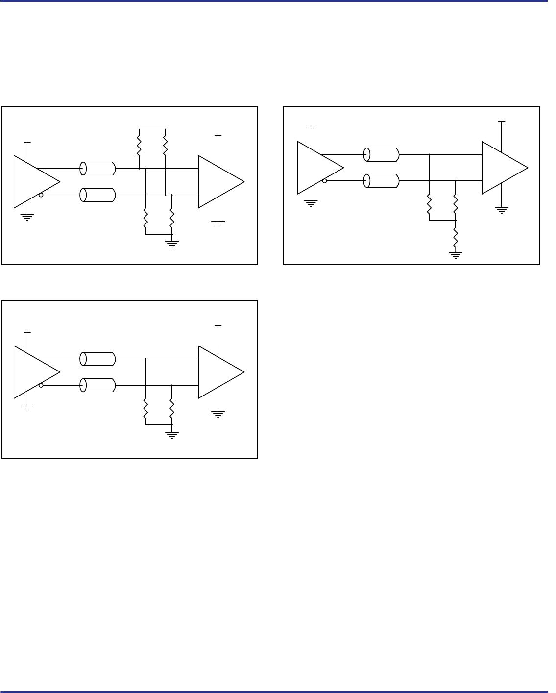
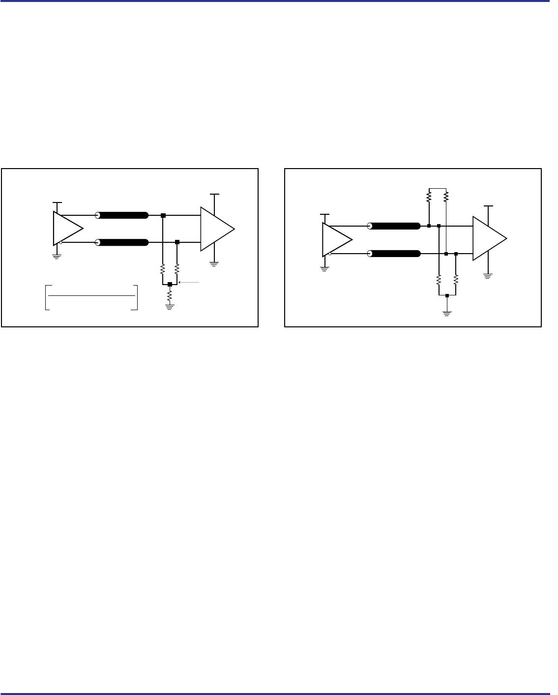
Termination for 3.3V LVPECL Outputs
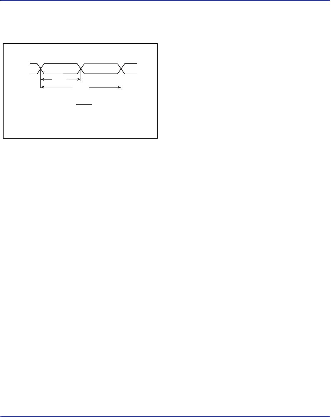
The clock layout topology shown below is a typical termination for
LVPECL outputs. The two different layouts mentioned are
recommended only as guidelines.
The differential outputs are low impedance follower outputs that
generate ECL/LVPECL compatible outputs. Therefore, terminating
resistors (DC current path to ground) or current sources must be
used for functionality. These outputs are designed to drive 50
transmission lines. Matched impedance techniques should be used
to maximize operating frequency and minimize signal distortion.
Figures 1A and 1B show two different layouts which are
recommended only as guidelines. Other suitable clock layouts may
exist and it would be recommended that the board designers
simulate to guarantee compatibility across all printed circuit and clock
component process variations.
Figure 1A. 3.3V LVPECL Output Termination Figure 1B. 3.3V LVPECL Output Termination
3.3V
V
CC
- 2V
R1
50Ω
R2
50Ω
RTT
Z
o
= 50Ω
Z
o
= 50Ω
+
_
RTT = * Z
o
1
((V
OH
+ V
OL
) / (V
CC
– 2)) – 2
3.3V
LVPECL
Input
R1
84Ω
R2
84Ω
3.3V
R3
125Ω
R4
125Ω
Z
o
= 50Ω
Z
o
= 50Ω
LVPECL Inp
ut
3.3V
3
.3V
+
_
IDT8N3Q001 REV G Data Sheet QUAD-FREQUENCY PROGRAMMABLE-XO
IDT8N3Q001GCD REVISION A
MARCH 6, 2012
12 ©2012 Integrated Device Technology, Inc.
Termination for 2.5V LVPECL Outputs
Figure 2A and Figure 2B show examples of termination for 2.5V
LVPECL driver. These terminations are equivalent to terminating 50
to V
CC
– 2V. For V
CC
= 2.5V, the V
CC
– 2V is very close to ground
level. The R3 in Figure 2B can be eliminated and the termination is
shown in Figure 2C.
Figure 2A. 2.5V LVPECL Driver Termination Example
Figure 2C. 2.5V LVPECL Driver Termination Example
Figure 2B. 2.5V LVPECL Driver Termination Example
2.5V LVPECL Driver
V
CC
= 2.5V
2.5V
2.5V
50Ω
50Ω
R1
250
Ω
R3
250
Ω
R2
62.5
Ω
R4
62.5
Ω
+
2.5V LVPECL Driver
V
CC
= 2.5V
2.5V
50Ω
50Ω
R1
50
Ω
R2
50
Ω
+
2.5V LVPECL Driver
V
CC
= 2.5V
2.5V
50Ω
50Ω
R1
50
Ω
R2
50
Ω
R3
18
Ω
+

8N3Q001FG-1053CDI

Mfr. #:
Manufacturer:
Description:
IC OSC CLOCK QD FREQ 10CLCC
Lifecycle:
New from this manufacturer.
Delivery:
DHL FedEx Ups TNT EMS
Payment:
T/T Paypal Visa MoneyGram Western Union