DATA SHEET
IDT8N3Q001GCD REVISION A
MARCH 6, 2012
1 ©2012 Integrated Device Technology, Inc.
Quad-Frequency Programmable XO IDT8N3Q001 REV G
General Description
The IDT8N3Q001 is a Quad-Frequency Programmable Clock
Oscillator with very flexible frequency programming capabilities. The
device uses IDT’s fourth generation FemtoClock® NG technology for
an optimum of high clock frequency and low phase noise
performance. The device accepts 2.5V or 3.3V supply and is
packaged in a small, lead-free (RoHS 6) 10-lead Ceramic 5mm x
7mm x 1.55mm package.
Besides the four default power-up frequencies set by the FSEL0 and
FSEL1 pins, the IDT8N3Q001 can be programmed via the I
2
C
interface to output clock frequencies between 15.476MHz to
866.67MHz and from 975MHz to 1,300MHz to a very high degree of
precision with a frequency step size of 435.9Hz ÷ N (N is the PLL
output divider). Since the FSEL0 and FSEL1 pins are mapped to 4
independent PLL M and N divider registers (P, MINT, MFRAC and N),
reprogramming those registers to other frequencies under control of
FSEL0 and FSEL1 is supported. The extended temperature range
supports wireless infrastructure, telecommunication and networking
end equipment requirements.
Features
• Fourth generation FemtoClock® NG technology
• Programmable clock output frequency from 15.476MHz to
866.67MHz and from 975MHz to 1,300MHz
• Four power-up default frequencies (see part number order
codes), re-programmable by I
2
C
• I
2
C programming interface for the output clock frequency and
internal PLL control registers
• Frequency programming resolution is 435.9Hz ÷N
• One 2.5V, 3.3V LVPECL clock output
• Two control inputs for the power-up default frequency
• LVCMOS/LVTTL compatible control inputs
• RMS phase jitter @ 156.25MHz (12kHz - 20MHz): 0.244ps
(typical), integer PLL feedback configuration
• RMS phase jitter @ 156.25MHz (1kHz - 40MHz): 0.265ps
(typical), integer PLL feedback configuration
• Full 2.5V or 3.3V supply modes
• -40°C to 85°C ambient operating temperature
• Available in Lead-free (RoHS 6) package
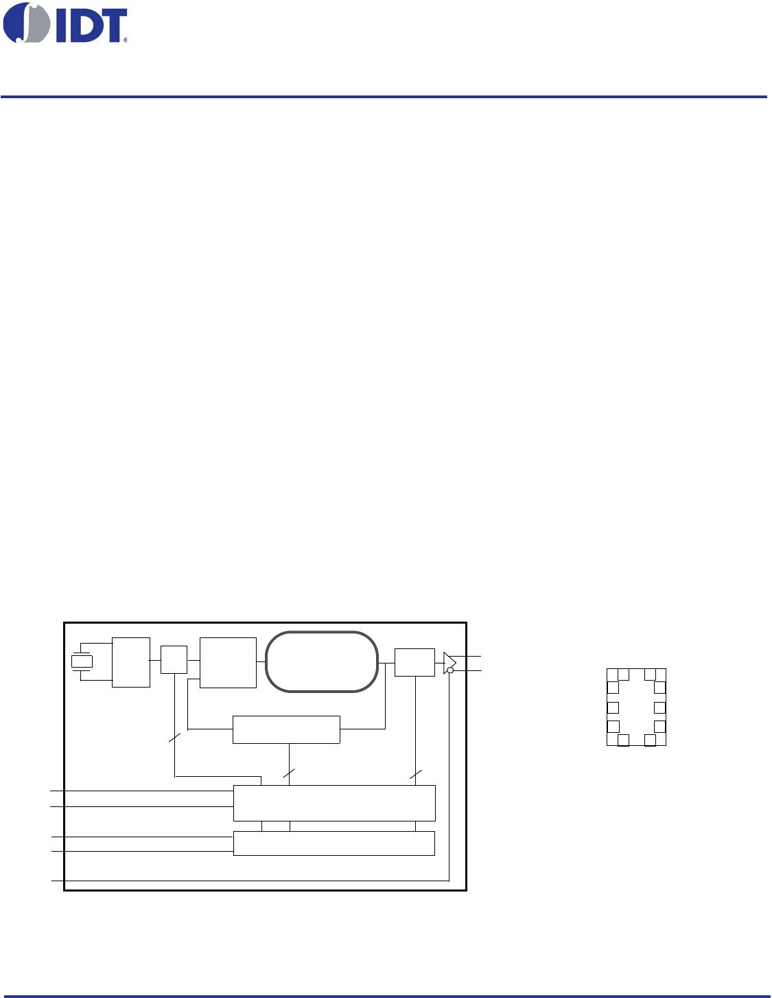
IDT8N3Q001
10-lead Ceramic 5mm x 7mm x 1.55mm
package body
CD Package
Top View
8 V
CC
7 nQ
6 Q
FSEL0 4
FSEL1 5
10 SCLK
9 SDATA
DNU 1
OE 2
V
EE
3
Pin Assignment
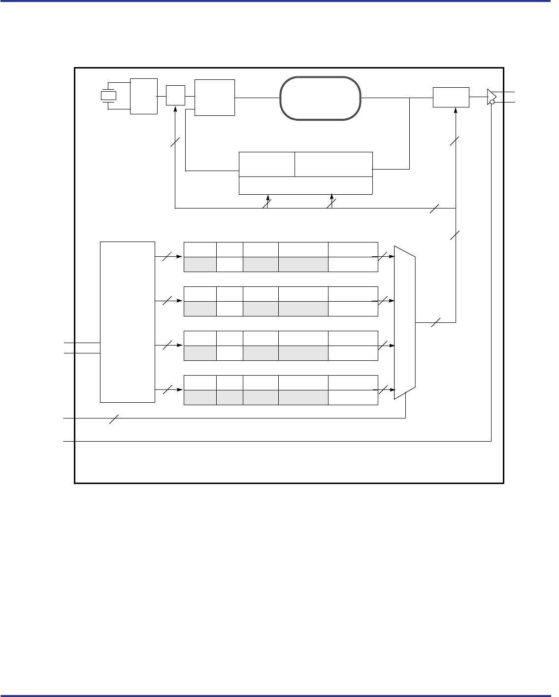
Block Diagram
Q
nQ
OSC
f
XTAL
÷MINT, MFRAC
PFD
&
LPF
FemtoClock® NG
VCO
1950-2600MHz
÷N
I
2
C Control
Configuration Register (ROM)
(Frequency, APR, Polarity)
25
7
FSEL1
FSEL0
SCLK
SDATA
OE
Pulldown
Pulldown
Pullup
Pullup
Pullup
÷P
2