The Smart Timing Choice
The Smart Timing Choice
SiTime Corporation 990 Almanor Avenue, Sunnyvale, CA 94085 (408) 328-4400 www.sitime.com
Rev. 1.7 Revised November 18, 2013
SiT9003
Low Power Spread Spectrum Oscillator
Features Applications
Frequency range from 1 MHz to 110 MHz Printers
LVCMOS/LVTTL compatible output Flat panel drivers
Standby current as low as 0.4 µA PCI
Fast resume time of 3 ms (Typ) Microprocessors
<30 ps cycle-to-cycle jitter
Spread options (contact SiTime for other spread options)
• Center spread: ±0.50%, ±0.25%
• Down spread: -1%, -0.5%
Standby, output enable, or spread disable mode
Industry-standard packages: 2.5 x 2.0, 3.2 x 2.5, 5.0 x 3.2,
7.0 x 5.0 mm x mm
Outstanding mechanical robustness for portable applications
All-silicon device with outstanding reliability of 2 FIT
(10x improvement over quartz-based devices), enhancing system
mean-time-to-failure (MTBF)
Pb-free, RoHS and REACH compliant
DC Electrical Characteristics
Parameters Symbol Min. Typ. Max. Unit Condition
Output Frequency Range f1–110MHz
Frequency Tolerance F_tol -50 – +50 PPM Inclusive of: Initial stability, operating temperature, rated power,
supply voltage change, load change, shock and vibration
Spread Off
-100 – +100 PPM
Aging Ag -1 – 1 PPM 1st year at 25°C
Operating Temperature Range T_use -20 – +70 °C Extended Commercial
-40 – +85 °C Industrial
Supply Voltage Vdd 1.71 1.8 1.89 V
2.25 2.5 2.75 V
2.52 2.8 3.08 V
2.97 3.3 3.63 V
Current Consumption Idd – 3.7 4.1 mA No load condition, f = 20 MHz, Vdd = 2.5 V, 2.8 V or 3.3 V
– 3.2 3.5 mA No load condition, f = 20 MHz, Vdd = 1.8 V
Standby Current I_std – 2.4 4.3
µAST = GND, Vdd = 3.3 V, Output is Weakly Pulled Down
–1.22.2
µAST = GND, Vdd = 2.5 or 2.8 V, Output is Weakly Pulled Down
–0.40.8
µAST = GND, Vdd = 1.8 V, Output is Weakly Pulled Down
Duty Cycle DC 45 – 55 % All Vdds. f <= 70 MHz
40 – 60 % All Vdds. f >70 MHz
Rise/Fall Time Tr, Tf – 1 2 ns 20% - 80% Vdd=2.5 V, 2.8 V or 3.3 V, 15 pf load
- 1.3 2.5 ns 20% - 80% Vdd=1.8 V, 15 pf load
Output Voltage High VOH 90% – – Vdd IOH = -4 mA (Vdd = 3.3 V)
IOH = -3 mA (Vdd = 2.8 V and 2.5 V)
IOH = -2 mA (Vdd = 1.8 V)
Output Voltage Low
VOL
– – 10 %Vdd IOL = -4 mA (Vdd = 3.3 V)
IOL = -3 mA (Vdd = 2.8 V and 2.5 V)
IOL = -2 mA (Vdd = 1.8 V)
Output Load Ld – – 15 pF At maximum frequency and supply voltage. Contact SiTime for
higher output load option
Input Voltage High VIH 70% – – Vdd Pin 1, OE or ST
or SD
Input Voltage Low VIL – – 30% Vdd Pin 1, OE or ST
or SD
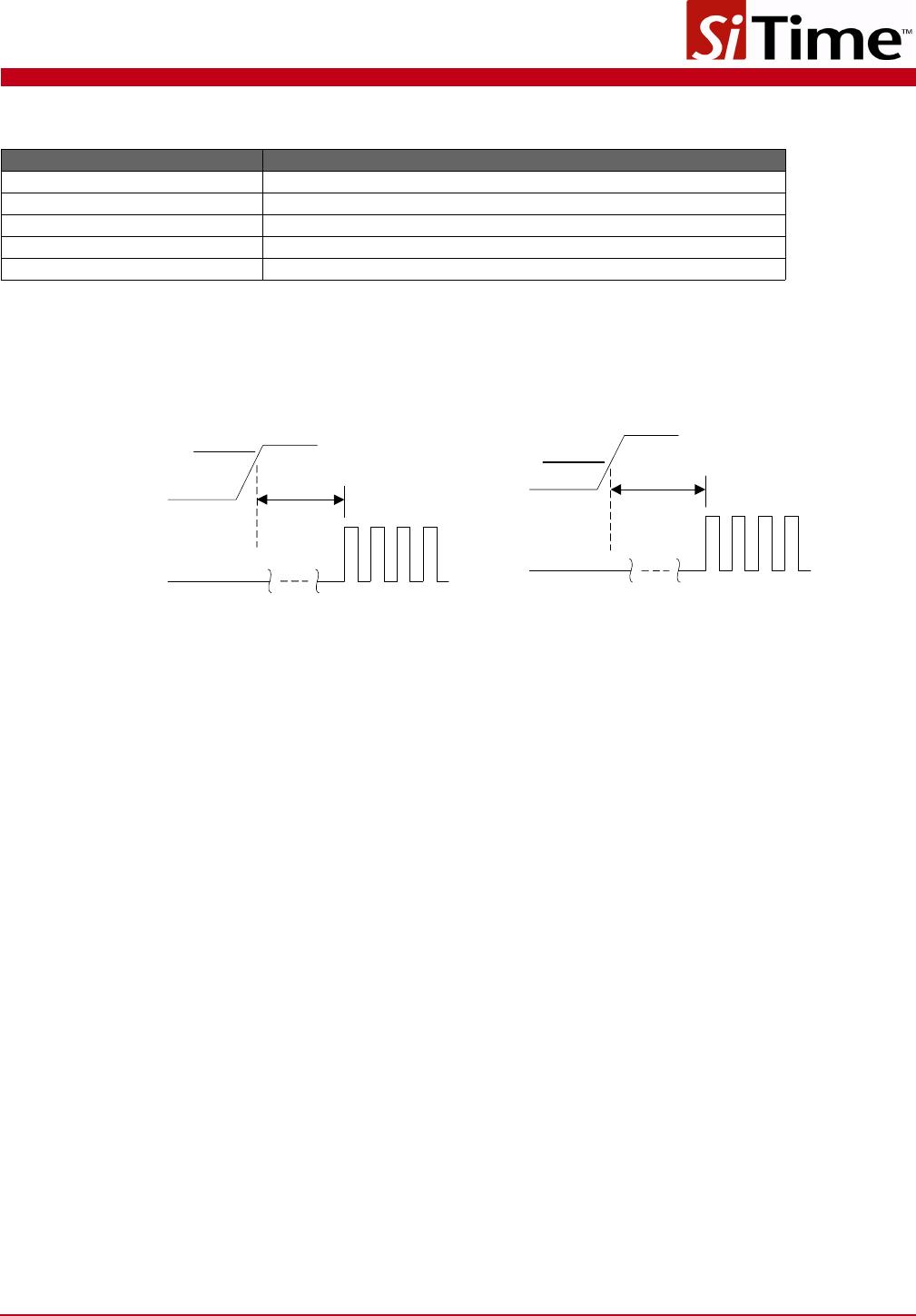
Startup Time T_start – – 10 ms Measured from the time Vdd reaches its rated minimum value
Resume Time T_resume – 3.0 3.8 ms Measured from the time ST pin crosses 50% threshold
Cycle-to-Cycle Jitter T_cyc – – 26 ps f = 50 MHz, Spread = ON
– – 26 ps f = 50 MHz, Spread = OFF