Data Sheet ADuM4120/ADuM4120-1
Rev. 0 | Page 7 of 17
ABSOLUTE MAXIMUM RATINGS
Ambient temperature = 25°C, unless otherwise noted.
Table 7.
Parameter Rating
Supply Voltages
V
DD1
− GND
1
−0.3 V to +7 V
V
DD2
− GND
2
−0.3 V to +40 V
Input Voltages
V
IN
1
− GND
1
−0.3 V to +7 V
Output Voltages
V
OUT
− GND
2
−0.3 V to V
DD2
+ 0.3 V
Common-Mode Transients (|CM|)
2
−200 kV/μs to +200 kV/μs
Storage Temperature Range (T
ST
) −55°C to +150°C
Ambient Operating Temperature
Range (T
A
)
−40°C to +125°C
1
Rating assumes V
DD1
is above 2.5 V. V
IN
is rated up to 6.5 V when V
DD1
is
unpowered.
2
|CM| refers to common-mode transients across the insulation barrier.
Common-mode transients exceeding the absolute maximum rating can
cause latch-up or permanent damage.
Stresses at or above those listed under Absolute Maximum
Ratings may cause permanent damage to the product. This is a
stress rating only; functional operation of the product at these
or any other conditions above those indicated in the operational
section of this specification is not implied. Operation beyond
the maximum operating conditions for extended periods may
affect product reliability.
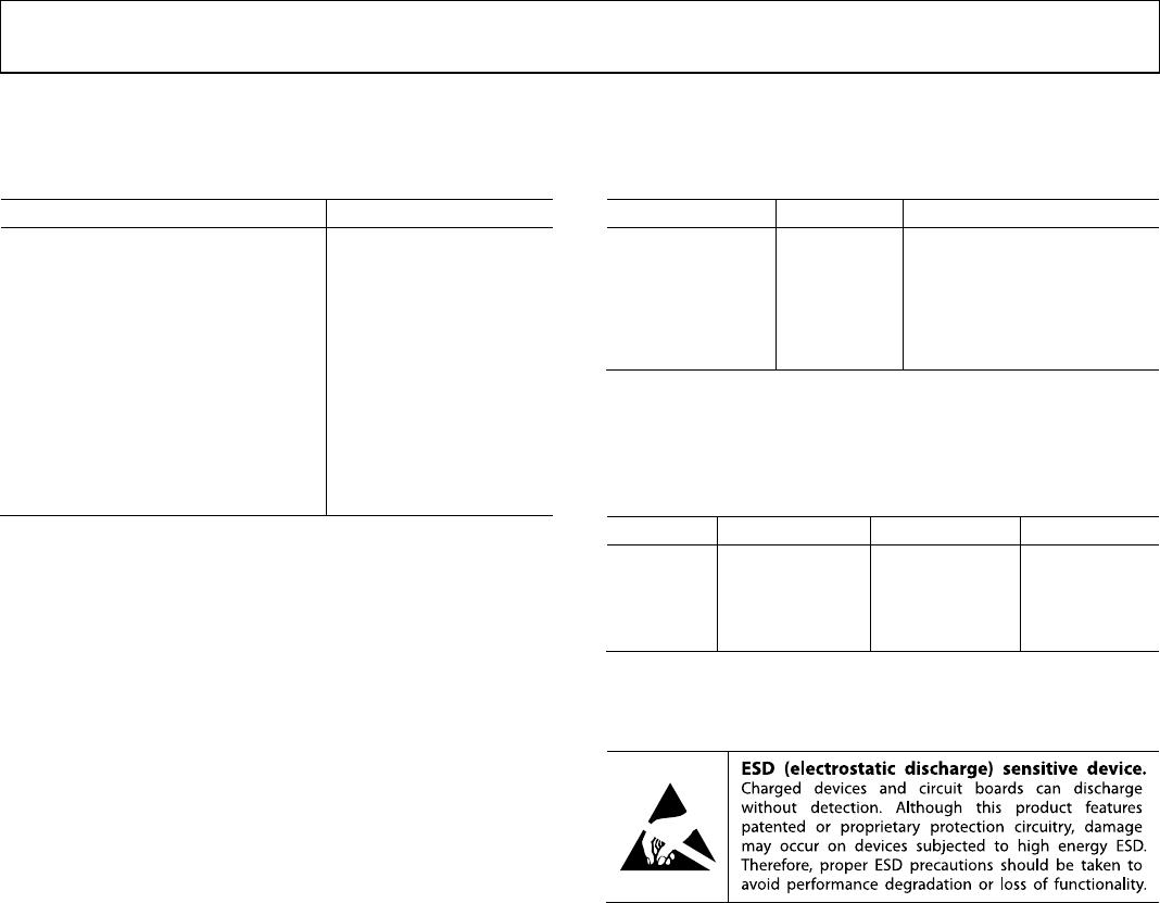
Table 8. ADuM4120/ADuM4120-1 Maximum Continuous
Working Voltage
1
Parameter Value Constraint
60 Hz AC Voltage 600 V rms
20-year lifetime at 0.1%
failure rate, zero average
voltage
DC Voltage 1092 V peak
Limited by the creepage of
the package, Pollution Degree
2, Material Group II
2, 3
1
See the Insulation Lifetime section for details.
2
Other pollution degree and material group requirements yield a different limit.
3
Some system level standards allow components to use the printed wiring
board (PWB) creepage values. The supported dc voltage may be higher for
those standards.
Table 9. Truth Table ADuM4120/ADuM4120-1 (Positive Logic)
V
IN
Input
1
V
DD1
State V
DD2
State V
OUT
Output
Low Powered Powered Low
High Powered Powered High
X Unpowered
2
Powered Low
X Powered Unpowered
2
High-Z
1
X means don’t care
2
Output returns within 20 μs of being powered.
ESD CAUTION