MILITARY AND INDUSTRIAL TEMPERATURE RANGES
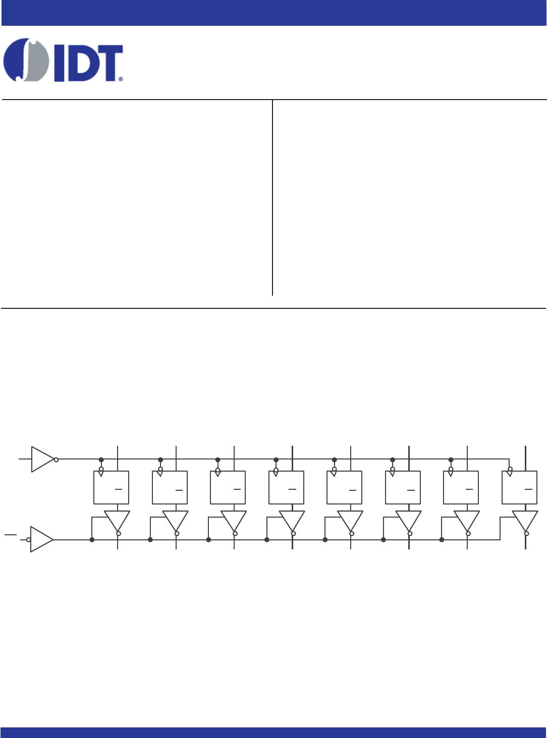
IDT54/74FCT574T/AT/CT
FAST CMOS OCTAL D REGISTERS (3-STATE)
3
NOTES:
1. For conditions shown as Min. or Max., use appropriate value specified under Electrical Characteristics for the applicable device type.
2. Typical values are at VCC = 5.0V, +25°C ambient.
3. Not more than one output should be tested at one time. Duration of the test should not exceed one second.
4. The test limit for this parameter is ±5µA at TA = –55°C.
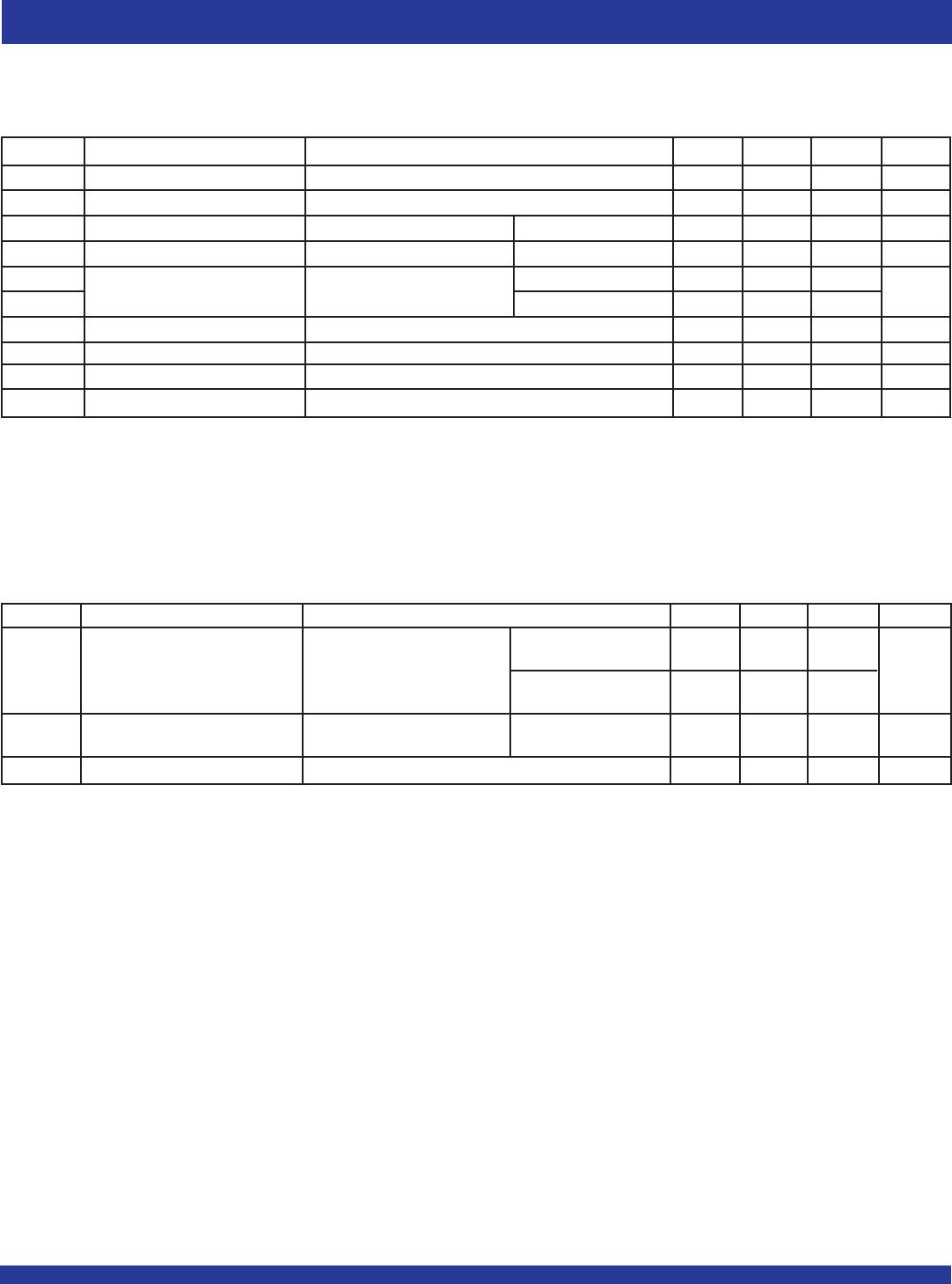
Symbol Parameter Test Conditions
(1)
Min. Typ.
(2)
Max. Unit
V
OH Output HIGH Voltage VCC = Min IOH = –6mA MIL 2.4 3.3 —
VIN = VIH or VIL IOH = –8mA IND V
IOH = –12mA MIL 2 3 —
IOH = –15mA IND
VOL Output LOW Voltage VCC = Min IOL = 32mA MIL — 0.3 0.5 V
VIN = VIH or VIL IOL = 48mA IND
IOS Short Circuit Current VCC = Max., VO = GND
(3)
–60 –120 –225 mA
OUTPUT DRIVE CHARACTERISTICS
Symbol Parameter Test Conditions
(1)
Min. Typ.
(2)
Max. Unit
VIH Input HIGH Level Guaranteed Logic HIGH Level 2 — — V
VIL Input LOW Level Guaranteed Logic LOW Level — — 0.8 V
IIH Input HIGH Current
(4)
VCC = Max. VI = 2.7V — — ±1µA
IIL Input LOW Current
(4)
VCC = Max. VI = 0.5V — — ±1µA
IOZH High Impedance Output Current VCC = Max VO = 2.7V — — ±1µA
IOZL (3-State output pins)
(4)
VO = 0.5V — — ±1
II Input HIGH Current
(4)
VCC = Max., VI = VCC (Max.) — — ±1µA
VIK Clamp Diode Voltage VCC = Min, IIN = -18mA — –0.7 –1.2 V
VH Input Hysteresis — — 200 — mV
I
CC Quiescent Power Supply Current VCC = Max., VIN = GND or VCC — 0.01 1 mA
DC ELECTRICAL CHARACTERISTICS OVER OPERATING RANGE
Following Conditions Apply Unless Otherwise Specified:
Industrial: TA = –40°C to +85°C, VCC = 5.0V ±5%; Military: TA = –55°C to +125°C, VCC = 5.0V ±10%