NCP302, NCP303
http://onsemi.com
21
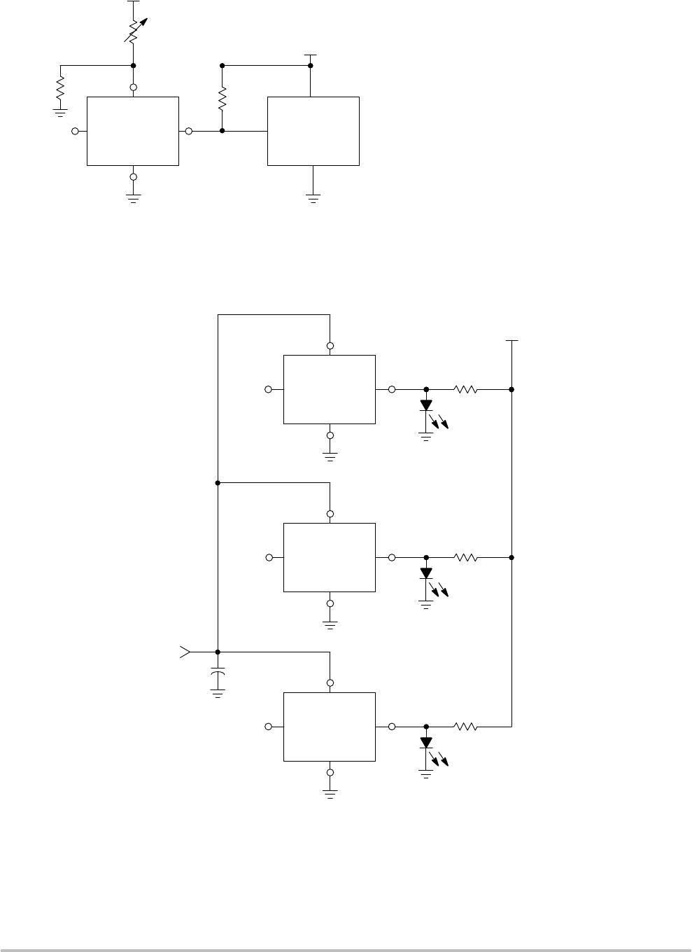
Figure 46. Multi−Rail Supply Undervoltage Monitor with Power Good
*
R1 is Optional C
D
Pin Pullup
3.3 V Power Supply 2
(I/O Subsystem)
V
IN
V
IN
0 V
0 V
0 V
V
TCD
C
D
Pin
Note: V
TCD
0.675 * V
IN
t
D2
2
1
5
3
Reset Output
Input
C
D
GND
NCP302L
Series
2
1
3
Reset Output
Input
GND
2
1
3
Reset Output
Input
GND
NCP301
LSN30T1
NCP301
LSN45T1
C
D
5.0 V Power Supply 3
(Peripheral Subsystem)
Power Supply 1
(System Core)
R1 R
P
*Required for
NCP303
To MCU or
Logic Circuitry
0 V
0 V
t
D2
t
D2
t
D2
Power Supply 1
Power Supply 2
V
P
Power Supply 3
NCP302L
RESET Output
This circuit monitors multiple power supply rails for
undervoltage conditions. If any of the three power supplies
are in an undervoltage condition, the NCP302 reset output
will be immediately set to an active low level. All three
power supplies must be above their minimum voltage levels
for the NCP302 reset output to generate a “Power Good”
level (Reset Output = Power Supply 1 or V
P
).
Optionally, R1 may be added to provide a smaller
effective C
D
pin pullup resistance, (R
D
’), where
R
D
’ = R1 || R
D
, with R
D
(internal C
D
pin pullup resistance)
approximately equal to 1.0 MW, and R1 > 5 kW. If R1 << R
D
,
then R1 also can decrease the reset output delay time (t
D2
)
variance over the operating temperature range.
The Power Good signal time delay (t
D2
) can be estimated
by: t
D2
≈ R
D
* C
D
, with R
D
in Ohms, and C
D
in Farads. If
R1 is installed, then R
D
’ is substituted for R
D
. R
P
is added
only if using the NCP303 to replace the NCP302. This
allows the Reset Output to be pulled up to V
P
, which can be
the Power Supply 1 or an independent power supply rail.