MAX535/MAX5351
Low-Power, 13-Bit Voltage-Output DACs
with Serial Interface
10 ______________________________________________________________________________________
Shutdown Mode
The MAX535/MAX5351 feature a software-programmable
shutdown that reduces supply current to a typical value
of 4µA. Writing 111XXXXXXXXXXXXX as the input-control
word puts the MAX535/MAX5351 in shutdown mode
(Table 1).
In shutdown mode, the MAX535/MAX5351 output ampli-
fier and the reference input enter a high-impedance
state. The serial interface remains active. Data in the
input registers is retained in shutdown, allowing the
MAX535/MAX5351 to recall the output state prior to
entering shutdown. Exit shutdown mode by either recall-
ing the previous configuration or by updating the DAC
with new data. When powering up the device or bringing
it out of shutdown, allow 20µs for the output to stabilize.
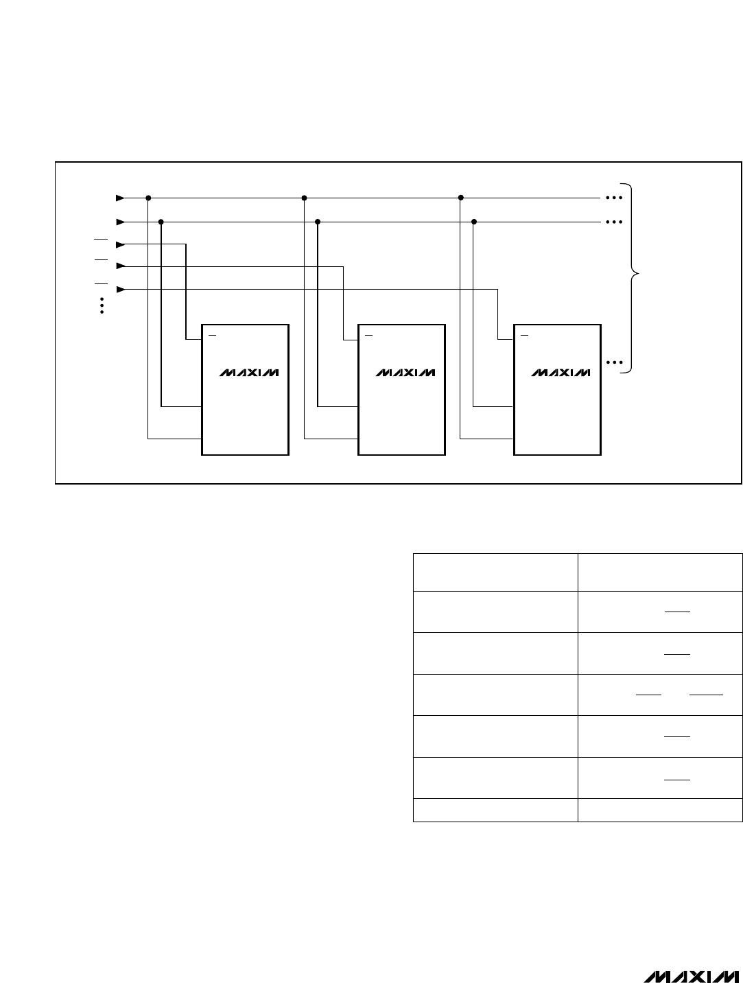
Serial-Interface Configurations
The MAX535/MAX5351’s 3-wire serial interface is com-
patible with both Microwire™ (Figure 2) and
SPI™/QSPI™ (Figure 3). The serial input word consists
of three control bits followed by 13 data bits (MSB first),
as shown in Figure 4. The 3-bit control code determines
the MAX535/MAX5351’s response outlined in Table 1.
The MAX535/MAX5351’s digital inputs are double
buffered. Depending on the command issued through
the serial interface, the input register can be loaded
without affecting the DAC register, the DAC register
can be loaded directly, or the DAC register can be
updated from the input register (Table 1).
Serial-Interface Description
The MAX535/MAX5351 require 16 bits of serial data.
Table 1 lists the serial-interface programming com-
mands. For certain commands, the 13 data bits are
“don’t cares.” Data is sent MSB first and can be sent in
two 8-bit packets or one 16-bit word (CS must remain
low until 16 bits are transferred). The serial data is com-
posed of three control bits (C2, C1, C0), followed by the
13 data bits D12...D0 (Figure 4). The 3-bit control code
determines:
The register to be updated
The configuration when exiting shutdown
Figure 5 shows the serial-interface timing requirements.
The chip-select pin (CS) must be low to enable the DAC’s
serial interface. When CS is high, the interface control cir-
cuitry is disabled. CS must go low at least t
CSS
before the
rising serial clock (SCLK) edge to properly clock in the
first bit. When CS is low, data is clocked into the internal
shift register via the serial-data input pin (DIN) on SCLK’s
rising edge. The maximum guaranteed clock frequency is
10MHz. Data is latched into the MAX535/MAX5351
input/DAC register on CS’s rising edge.
SCLK
DIN
CS
SK
SO
I/O
MAX535
MAX5351
MICROWIRE
PORT
Figure 2. Connections for Microwire
DIN
SCLK
CS
MOSI
SCK
I/O
SPI/QSPI
PORT
SS
+5V
CPOL = 0,CPHA = 0
MAX535
MAX5351
Figure 3. Connections for SPI/QSPI
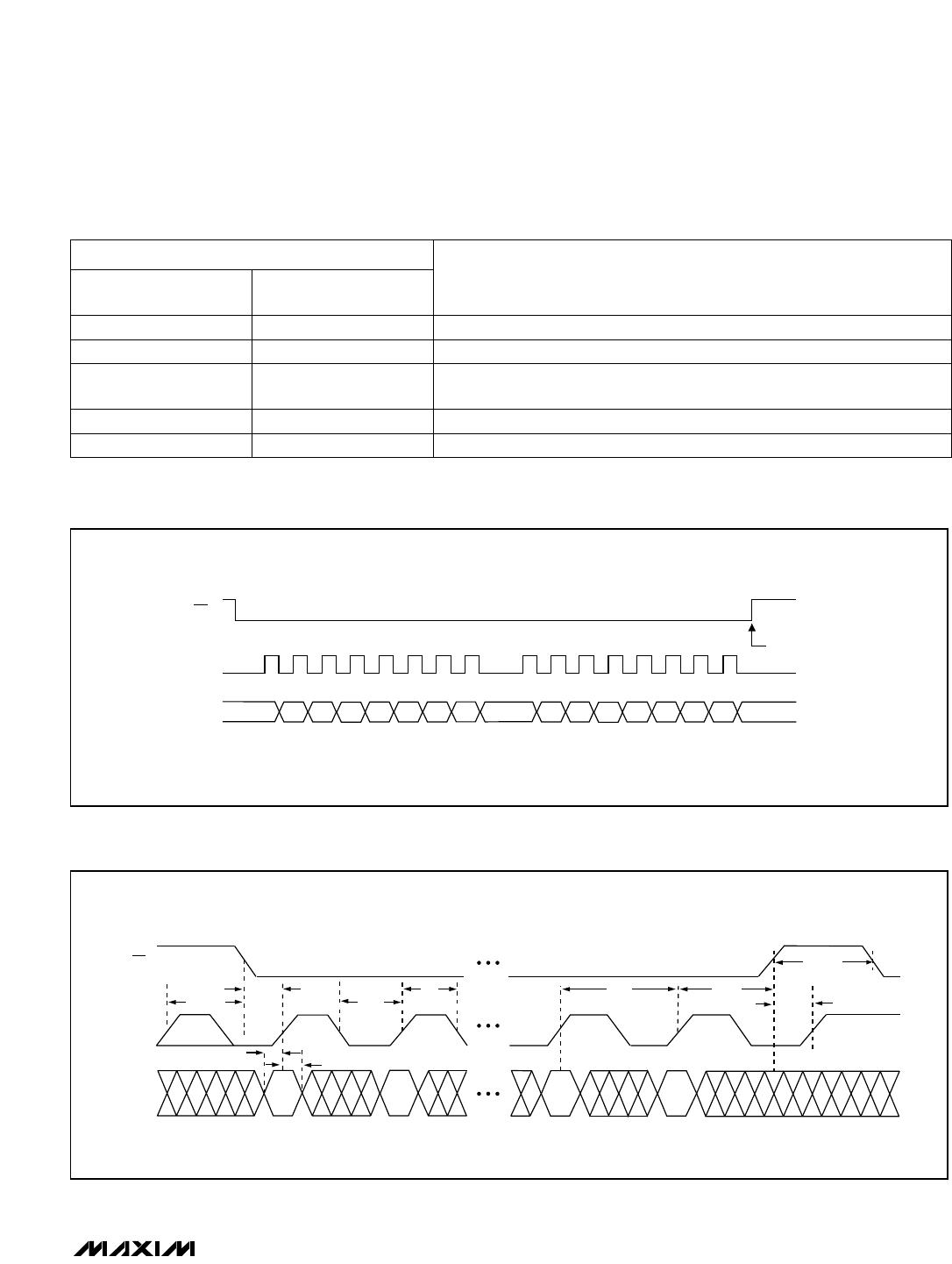
Figure 4. Serial-Data Format
3 Control
Bits
13 Data Bits
D12................................................D0C2 C1 C0
Data Bits
MSB.............................................LSB
Control
Bits
16 Bits of Serial Data
MSB..................................................................................LSB
MAX535/MAX5351
Low-Power, 13-Bit Voltage-Output DACs
with Serial Interface
______________________________________________________________________________________ 11
CS
SCLK
DIN
COMMAND
EXECUTED
9
8
16
1
C1
C2 D0
C0
D12
D11
D10
D9 D6 D5 D4 D3 D2 D1D8 D7
Figure 5. Serial-Interface Timing Diagram
Figure 6. Detailed Serial-Interface Timing Diagram
Table 1. Serial-Interface Programming Commands
“X” = Don’t care
XXXXXXXXXXXXX
XXXXXXXXXXXXX
13 bits of data
13 bits of data
XXXXXXXXXXXXX
Shutdown
Update DAC register from input register (also exit shutdown; recall previ-
ous state).
C2 C1 C0
Load input register; DAC register unchanged.
FUNCTION
D12............................D0
MSB LSB
Load input register; DAC register immediately updated (also exit shutdown).
No operation (NOP)
11 1
X1 0
X0 1
X0 0
01 1
16-BIT SERIAL WORD
SCLK
DIN
t
CSO
t
CSS
t
CL
t
CH
t
CP
t
CSW
t
CS1
t
CSH
t
DS
t
DH
CS
MAX535/MAX5351
Low-Power, 13-Bit Voltage-Output DACs
with Serial Interface
12 ______________________________________________________________________________________
Figure 7 shows a method of connecting several
MAX535/MAX5351s. In this configuration, the clock and
the data bus are common to all devices and separate
chip-select lines are used for each IC.
__________Applications Information
Unipolar Output
For a unipolar output, the output voltage and the refer-
ence input have the same polarity. Figure 8 shows the
MAX535/MAX5351 unipolar output circuit, which is also
the typical operating circuit. Table 2 lists the unipolar
output codes.
For rail-to-rail output, see Figure 9. This circuit shows
the MAX535/MAX5351 with the output amplifier config-
ured with a closed-loop gain of +2 to provide 0V to 5V
full-scale range when a 2.5V reference is used. When
using the MAX5351 with a 1.25V reference, this circuit
provides a 0V to 2.5V full-scale range.
Bipolar Output
The MAX535/MAX5351 output can be configured for
bipolar operation using Figure 10’s circuit.
V
OUT
= V
REF
[(2NB / 8192) - 1]
where NB is the numeric value of the DAC’s binary input
code. Table 3 shows digital codes (offset binary) and
the corresponding output voltage for Figure 10’s circuit.
Using an AC Reference
In applications where the reference has AC-signal com-
ponents, the MAX535/MAX5351 have multiplying capa-
bility within the reference input range specifications.
Figure 11 shows a technique for applying a sine-wave
signal to the reference input where the AC signal is off-
set before being applied to REF. The reference voltage
must never be more negative than GND.
TO OTHER 
SERIAL DEVICES
MAX535
MAX5351
DIN
SCLK
CS
MAX535
MAX5351
DIN
SCLK
CS
MAX535
MAX5351
DIN
SCLK
CS
DIN
SCLK
CS1
CS2
CS3
Figure 7. Multiple MAX535/MAX5351s Sharing Common DIN and SCLK Lines
Table 2. Unipolar Code Table
ANALOG OUTPUT
11111 1111 1111
10000 0000 0001
DAC CONTENTS
MSB LSB
10000 0000 0000
01111 1111 1111
00000 0000 0000 0V
00000 0000 0001
+V
8191
8192
REF
+V
4097
8192
REF
+V
4096
8192
REF
=
+
V
REF
2
+V
4095
8192
REF
+V
1
8192
REF

MAX5351AEUA+

Mfr. #:
Manufacturer:
Maxim Integrated
Description:
Digital to Analog Converters - DAC 13-Bit Precision DAC
Lifecycle:
New from this manufacturer.
Delivery:
DHL FedEx Ups TNT EMS
Payment:
T/T Paypal Visa MoneyGram Western Union