VS-209CNQ...PbF Series
www.vishay.com
Vishay Semiconductors
Revision: 23-Sep-15
1
Document Number: 94156
For technical questions within your region: DiodesAmericas@vishay.com
, DiodesAsia@vishay.com, DiodesEurope@vishay.com
THIS DOCUMENT IS SUBJECT TO CHANGE WITHOUT NOTICE. THE PRODUCTS DESCRIBED HEREIN AND THIS DOCUMENT
ARE SUBJECT TO SPECIFIC DISCLAIMERS, SET FORTH AT www.vishay.com/doc?91000
High Performance Schottky Rectifier, 200 A
FEATURES
• 175 °C T
J
operation
• Center tap module
• Low forward voltage drop
• High frequency operation
• Guard ring for enhanced ruggedness and long term
reliability
• UL approved file E222165
• Designed and qualified for industrial level
• Material categorization: for definitions of compliance
please see www.vishay.com/doc?99912
DESCRIPTION / APPLICATIONS
The VS-209CNQ center tap Schottky rectifier module series
has been optimized for low reverse leakage at high
temperature. The proprietary barrier technology allows for
reliable operation up to 175 °C junction temperature. Typical
applications are in high current switching power supplies,
plating power supplies, UPS systems, converters,
freewheeling diodes, welding, and reverse battery
protection.
PRODUCT SUMMARY
I
F(AV)
200 A
V
R
135 V, 150 V
Package TO-244
Circuit Two diodes common cathode
Base common
cathode
Lug
terminal
anode 1
Lug
terminal
anode 2
TO-244
MAJOR RATINGS AND CHARACTERISTICS
SYMBOL CHARACTERISTICS VALUES UNITS
I
F(AV)
Rectangular waveform 200 A
V
RRM
Range 135/150 V
I
FSM
t
p
= 5 μs sine 10 000 A
V
F
100 A
pk
, T
J
= 125 °C (per leg) 0.71 V
T
J
Range -55 to +175 °C
VOLTAGE RATINGS
PARAMETER SYMBOL VS-209CNQ135PbF VS-209CNQ150PbF UNITS
Maximum DC reverse voltage V
R
135 150 V
Maximum working peak reverse voltage V
RWM
ABSOLUTE MAXIMUM RATINGS
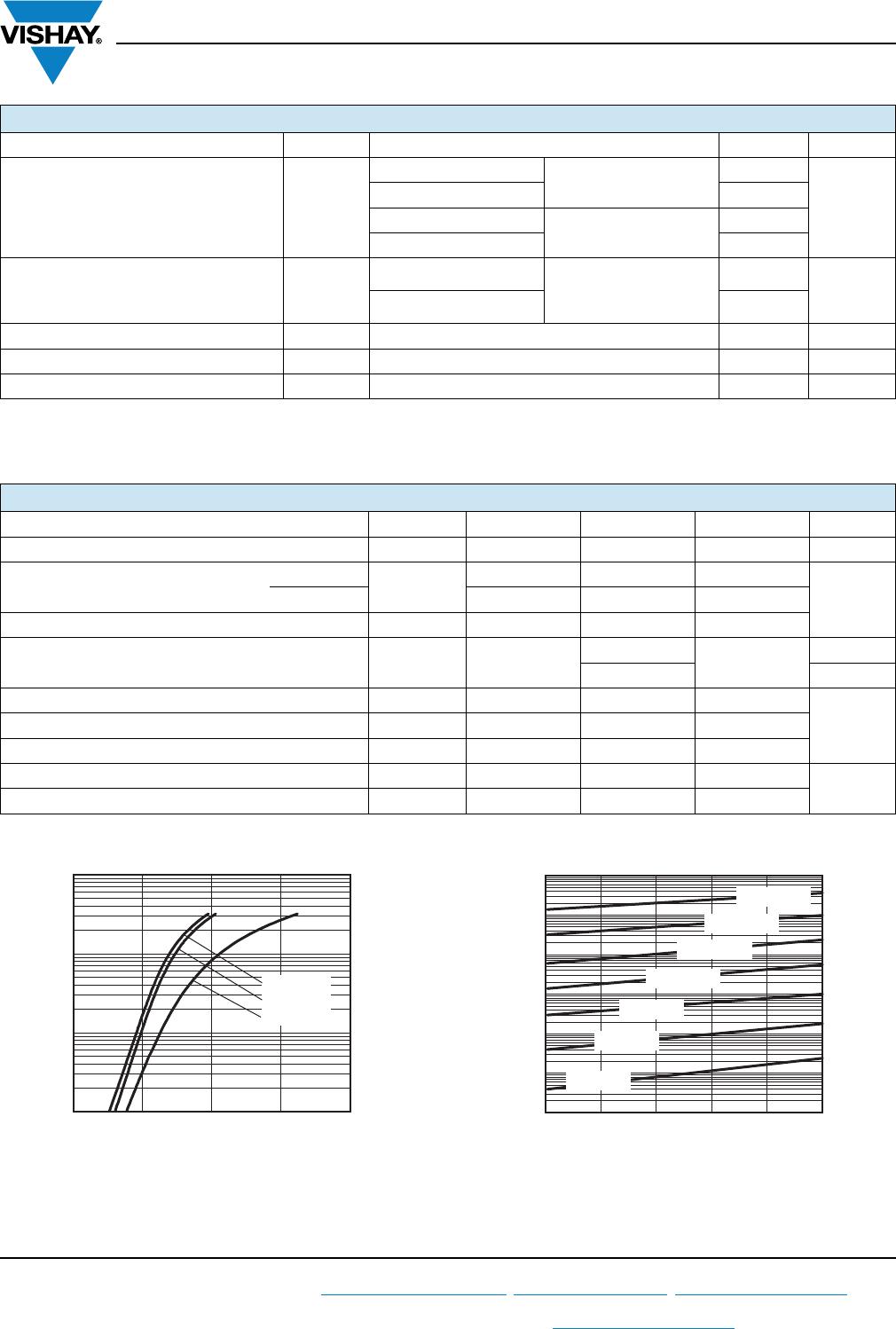
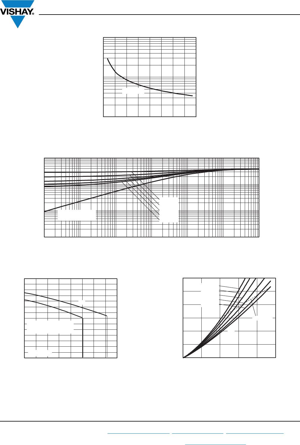
PARAMETER SYMBOL TEST CONDITIONS VALUES UNITS
Maximum average forward current
See fig. 5
per leg
I
F(AV)
50 % duty cycle at T
C
= 131 °C, rectangular
waveform
100
A
per device 200
Maximum peak one cycle non-repetitive surge
current per leg
See fig. 7
I
FSM
5 μs sine or 3 μs rect. pulse
Following any rated
load condition and
with rated V
RRM
applied
10 000
10 ms sine or 6 ms rect. pulse 1200
Non-repetitive avalanche energy per leg E
AS
T
J
= 25 °C, I
AS
= 5.5 A, L = 1 mH 15 mJ
Repetitive avalanche current per leg I
AR
Current decaying linearly to zero in 1 μs
Frequency limited by T
J
maximum V
A
= 1.5 x V
R
typical
1A