Data Sheet AD8307
Rev. E | Page 21 of 24
1 μW TO 1 kW 50 Ω POWER METER
The front-end adaptation shown in Figure 41 provides the
measurement of power being delivered from a transmitter final
amplifier to an antenna. The range has been set to cover the
power range −30 dBm (7.07 mV rms, or 1 W) to +60 dBm
(223 V rms, or 1 kW). A nominal voltage attenuation ratio of
158:1 (44 dB) is used; thus the intercept is moved from −84 dBm to
−40 dBm and the AD8307, scaled 0.25 V/decade of power, now
reads 1.5 V for a power level of 100 mW, 2.0 V at 10 W, and
2.5 V at 1 kW. The general expression is
P (dBm) = 40 (V
OUT
− 1)
The required attenuation can be implemented using a capacitive
divider, providing a very low input capacitance, but it is difficult to
ensure accurate values of small capacitors. A better approach is
to use a resistive divider, taking the required precautions to minim-
ize spurious coupling into the AD8307 by placing it in a shielded
box with the input resistor passing through a hole in this box, as
indicated in Figure 41. The coupling capacitors shown in Figure 41
are suitable for f ≥ 10 MHz. A capacitor can be added across the
input pins of the AD8307 to reduce the response to spurious HF
signals, which, as previously noted, extends to over 1 GHz.
The mismatch caused by the loading of this resistor is trivial;
only 0.05% of the power delivered to the load is absorbed by the
measurement system, a maximum of 500 mW at 1 kW. The
postdemodulation filtering and slope calibration arrangements
are chosen from other applications described in this data sheet
to meet the particular system requirements. The 1 nF capacitor
lowers the risk of HF signals entering the AD8307 via the load.
TO
NTENN
V
P
604Ω
100kΩ
1/2W
NC
2kΩ
VR1
2kΩ
INT ±3dB
51pF
51pF
0.1µF
NC
OUTPUT
LEAD-
THROUGH
CAPACITORS,
1nF
1nF
NC = NO CONNECT
+5V
V
OUT
01082-041
AD8307
INP VPS ENB INT
INM COM OFS OUT
8765
234
1
50Ω INPUT
FROM P.A.
1µW TO
1kW
22Ω
Figure 41. 1 μW to 1 kW, 50 Ω Power Meter
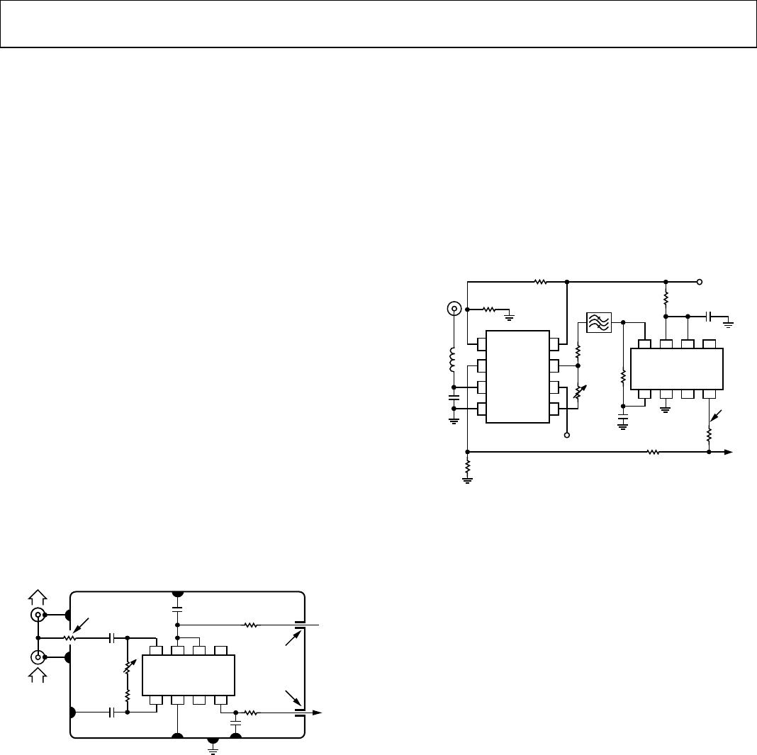
MEASUREMENT SYSTEM WITH 120 dB DYNAMIC
RANGE
The dynamic range of the AD8307 can be extended further from
90 dB to over 120 dB by the addition of an X-AMP® such as the
AD603. This type of variable gain amplifier exhibits a very exact
exponential gain control characteristic, which is another way of
stating that the gain varies by a constant number of decibels for
a given change in the control voltage. For the AD603, this scaling
factor is 40 dB/V, or 25 mV/dB. It is apparent that this property
of a linear-in-dB response is characteristic of log amps; indeed,
the AD8307 exhibits the same scaling factor.
The AD603 has a very low input-referred noise: 1.3 nV/√Hz at its
100 input, or 0.9 nV/√Hz when matched to 50 , equivalent to
0.4 V rms, or −115 dBm, in a 200 kHz bandwidth. It is also
capable of handling inputs in excess of 1.4 V rms, or +16 dBm. It is
thus able to cope with a dynamic range of over 130 dB in this
particular bandwidth.
If the gain control voltage for the X-AMP is derived from the
output of the AD8307, the effect is to raise the gain of this front-
end stage when the signal is small and lower it when it is large,
but without altering the fundamental logarithmic nature of the
response. This gain range is 40 dB, which, combined with the 90 dB
range of the AD8307, again corresponds to a 130 dB range.
VPOS
GNEG
AD603
FDBK
GPOS
VNEG
COMM
VINP
VOUT
0.65V
0.15V TO 1.15V
OUTPUT
10mV/dB
NC
R6
20kΩ
R7
80.6kΩ
0.1µF
BANDPASS
FILTER*
VR1
5kΩ
INT
±8dB
1nF
NC
0.3V
TO
2.3V
C1
150pF
L1
750nH
R3
330Ω
R4
464Ω
R5
100kΩ
*FOR EXAMPLE: MURATA SFE10.7MS2G-A
NC = NO CONNECT
50Ω
INPUT
–105dBm
TO
+15dBm
1
2
3
4
8
7
6
5
R2
28kΩ
R1
187kΩ
4.7Ω
AD8307
INP VPS ENB INT
INM COM OFS OUT
8765
234
1
V
N
, –5V
P
, +5
01082-042
Figure 42. 120 dB Measurement System
Figure 42 shows how these two parts can work together to
provide state-of-the-art IF measurements in applications such
as spectrum/network analyzers and other high dynamic range
instrumentation. To understand the operation, note first that
the AD8307 is used to generate an output of about 0.3 V to
2.3 V. This 2 V span is divided by 2 in R5, R6, and R7 to provide
the 1 V span needed by the AD603 to vary its gain by 40 dB.
Note that an increase in the positive voltage applied at GNEG
(Pin 2 of the AD603) lowers the gain. This feedback network is
tapped to provide a convenient 10 mV/dB scaling at the output
node, which can be buffered if necessary.
The center of the voltage range fed back to the AD603 is 650 mV,
and the ±20 dB gain range is centered by R1/R2. Note that the
intercept calibration of this system benefits from the use of a
well-regulated 5 V supply. To absorb the insertion loss of the
filter and center the full dynamic range, the intercept is adjusted
by varying the maximum gain of the AD603, using VR1. Figure 43
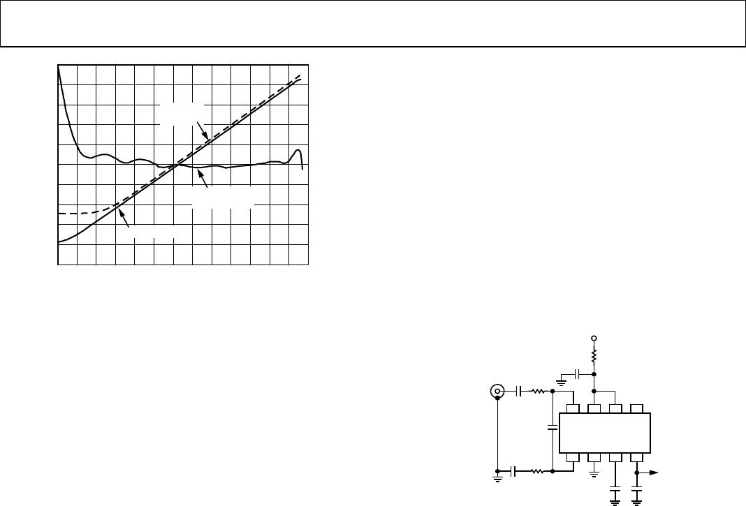
shows the AD8307 output over the range −120 dBm to +20 dBm
and the deviation from an ideal logarithmic response. The
dotted line shows the increase in the noise floor that results when
the filter is omitted; the decibel difference is about 10 log
10
(50/0.2)
or 24 dB, assuming a 50 MHz bandwidth from the AD603. An
LC filter can be used in place of the ceramic filter used in this
example.