7
LTC1051/LTC1053
10513fa
As the ambient temperature rises, the leakage current of
the input protection devices increases, while the charge
injection component of the bias current, for all practical
purposes, stays constant. At elevated temperatures (above
85°C) the leakage current dominates and the bias current
of both inputs assumes the same sign.
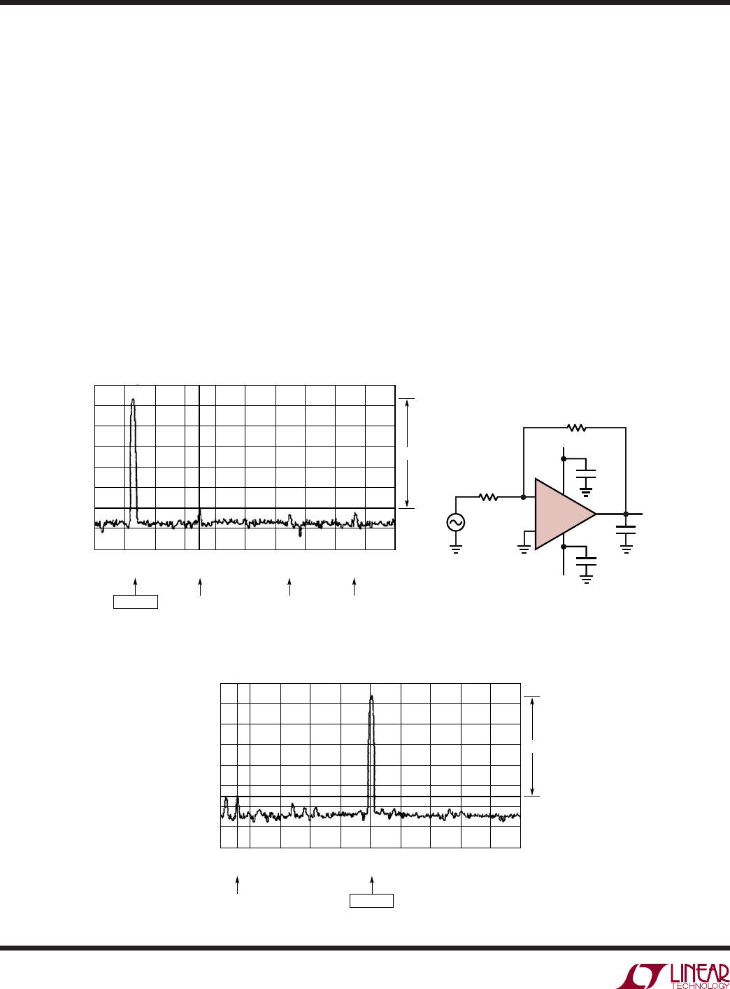
The charge injection at the op amp input pins will cause
small output spikes. This phenomenon is often referred to
as “clock feedthrough” and can be easily observed when
the closed-loop gain exceeds 10V/V (Figure 2). The mag-
nitude of the clock feedthrough is temperature indepen-
dent but it increases when the closed-loop gain goes up,
when the source resistance increases and when the gain
setting resistors increase (Figure 2a, 2b). It is important to
note that the output small spikes are centered at 0V level
and do not add to the output offset error budget. For
instance, with R
S
= 1MΩ, the typical output offset voltage
of Figure 2c is:
V
OS(OUT)
≈ 10
8
• I
B
+
+ 101V
OS(IN)
A 10pA bias current will yield an output of 1mV ±100µV.
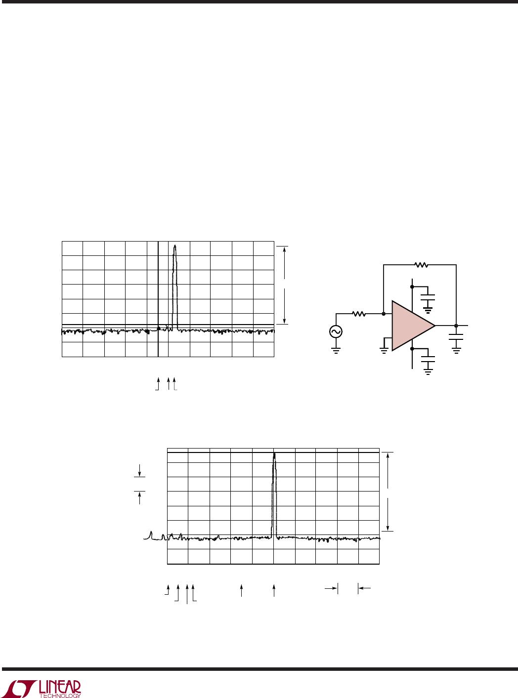
The output clock feedthrough can be attenuated by lower-
ing the value of the gain setting resistors, i.e. R2 = 10k,
R1 = 100Ω, instead of 100k and 1k (Figure 2).
Clock feedthrough can also be attenuated by adding a
capacitor across the feedback resistor to limit the circuit
bandwidth below the internal sampling frequency
(Figure 3).
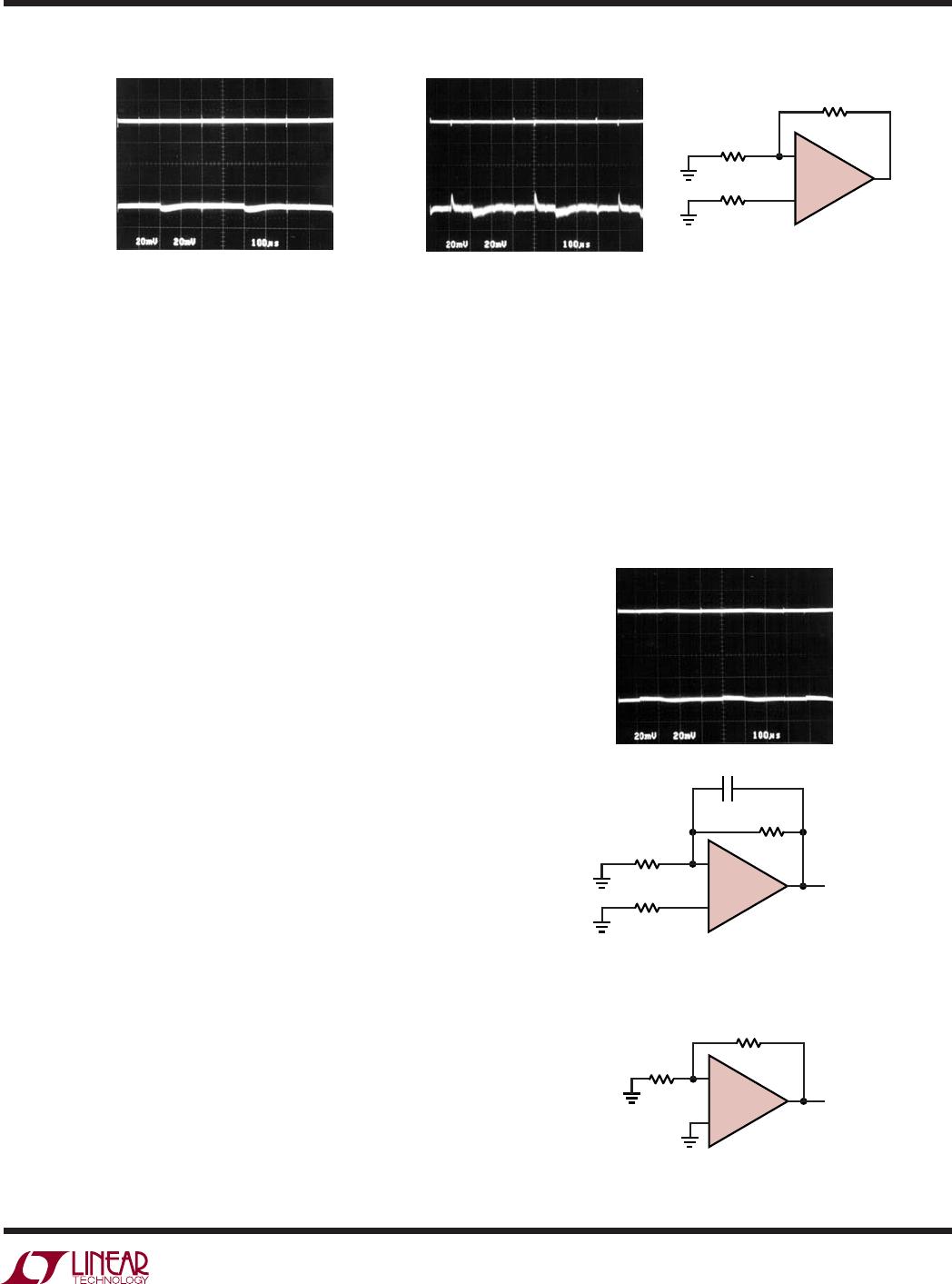
Input Capacitance
The input capacitance of the LTC1051/LTC1053 op amps
is approximately 12pF. When the LTC1051/LTC1053 op
amps are used with feedback factors approaching unity,
the feedback resistor value should not exceed 7k for
industrial temperature range and 5k for military tempera-
ture range. If a higher feedback resistor value is required,
a feedback capacitor of 20pF should be placed across the
feedback resistor. Note that the most common circuits
with feedback factors approaching unity are unity gain
followers and instrumentation amplifier front ends.
(See Figure 4.)
Figure 2. Clock Feedthrough
Figure 3. Adding a Feedback Capacitor to
Eliminate Clock Feedthrough
–
+
1/2
LTC1051
R
S
1051/53 F02
(c)
100µs/DIV
(b)
100µs/DIV
(a)
R1
1k
R2
100k
R
S
= 0,
A
V
=11V/V
20mV/DIV
R
S
= 0,
A
V
=101V/V
20mV/DIV
R
S
= 100k,
A
V
=11V/V
20mV/DIV
R
S
= 100k,
A
V
=101V/V
20mV/DIV
Figure 4. Operating the LTC1051
with Feedback Factors Approaching Unity
–
+
1/2
LTC1051
1051/53 F04
R1
R2 < 7k, IF R1 > >R2
1
2
3
–
+
1/2
LTC1051
R
S
1051/53 F03
R1
1k
R2
100k
C
1000pF
1
2
3
100µs/DIV
R
S
= 100k
A
V
=101V/V
R
S
= 1MΩ
A
V
=101V/V
20mV/DIV
APPLICATIO S I FOR ATIO
WUUU