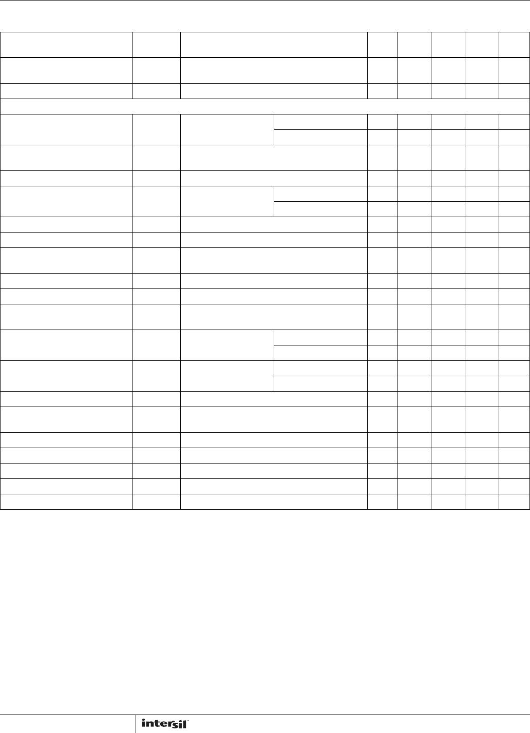
4
Driver Short-Circuit Current,
V
O
= High or Low
I
OSD1
DE = V
CC
, -7V V
Y
or V
Z
12V (Note 4) Full 60 - 250 mA
Receiver Short-Circuit Current I
OSR
0V V
O
V
CC
Full 7 - 85 mA
SWITCHING CHARACTERISTICS
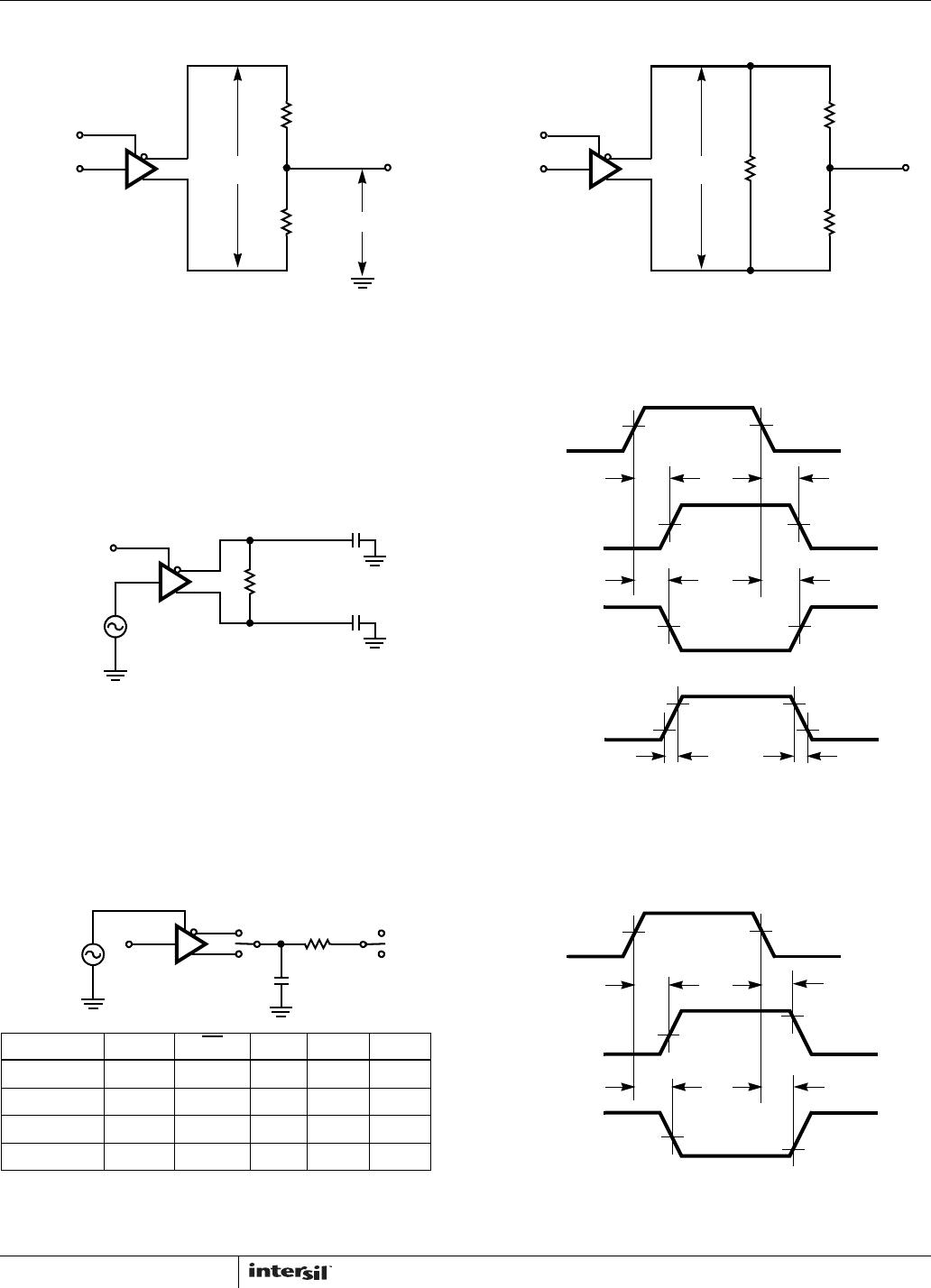
Driver Input to Output Prop Delay t
PLH
, t
PHL
R
DIFF
= 54,
C
L
= 100pF (Figure 2)
ISL4486 Full 3 9 14 ns
ISL81486 Full 3 9 17 ns
Prop Delay Delta, Min-to-Max t
DP-PSKEW
R
DIFF
= 54, C
L
= 100pF, ISL4486 Only (Note 6,
Figure 2)
Full - 0 6 ns
Driver Prop Delay Skew t
SKEW
R
DIFF
= 54, C
L
= 100pF (Figure 2) Full - 0 2 ns
Driver Differential Rise or Fall Time t
R
, t
F
R
DIFF
= 54,
C
L
= 100pF (Figure 2)
ISL4486 Full - 5 8 ns
ISL81486 Full - 7 15 ns
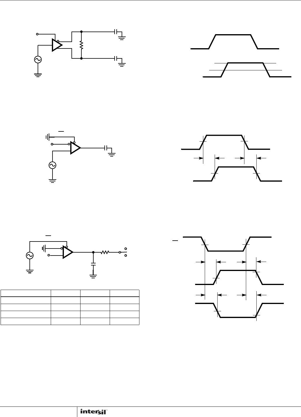
Driver Enable to Output High t
ZH
C
L
= 50pF, SW = GND (Figure 3) Full - 9 15 ns
Driver Enable to Output Low t
ZL
C
L
= 50pF, SW = V
CC
(Figure 3) Full - 9 15 ns
Matched Enable Switching
|t
AZH
- t
BZL
| or |t
BZH
- t
AZL
|
t
EN
At Identical Test Conditions (Figure 3) Full - 1 3 ns
Driver Disable from Output High t
HZ
C
L
= 50pF, SW = GND (Figure 3) Full - 9 15 ns
Driver Disable from Output Low t
LZ
C
L
= 50pF, SW = V
CC
(Figure 3) Full - 9 15 ns
Matched Disable Switching
|t
AHZ
- t
BLZ
| or |t
BHZ
- t
ALZ
|
t
DIS
At Identical Test Conditions (Figure 3) Full - 2 5 ns
Driver Maximum Data Rate f
MAXD
V
OD
| 1.5V (Figure 4) ISL4486 Full 40 - - Mbps
ISL81486 Full 30 - - Mbps
Receiver Input to Output Prop
Delay
t
PLH
, t
PHL
(Figure 5) ISL4486 Full 11 17 25 ns
ISL81486 Full 6 17 25 ns
Prop Delay Delta, Min-to-Max t
RP-PSKEW
ISL4486 Only (Note 6, Figure 5) Full - 0 9 ns
Receiver Prop Delay Skew
| t
PLH
- t
PHL
|
t
SKD
Figure 5 Full - 0.5 3 ns
Receiver Enable to Output High t
ZH
C
L
= 15pF, SW = GND (Figure 6) Full - 7 13 ns
Receiver Enable to Output Low t
ZL
C
L
= 15pF, SW = V
CC
(Figure 6) Full - 7 13 ns
Receiver Disable from Output High t
HZ
C
L
= 15pF, SW = GND (Figure 6) Full - 7 13 ns
Receiver Disable from Output Low t
LZ
C
L
= 15pF, SW = V
CC
(Figure 6) Full - 7 13 ns
Receiver Maximum Data Rate f
MAXR
C
L
= 15pF, V
ID
1.5V, RO t
H
and t
L
20ns Full 40 - - Mbps
NOTES:
2. All currents into device pins are positive; all currents out of device pins are negative. All voltages are referenced to device ground unless
otherwise specified.
3. Supply current specification is valid for loaded drivers when DE = 0V.
4. Applies to peak current. See “Typical Performance Curves” for more information.
5. Devices meeting these limits are denoted as “0.6 unit load (UL)” transceivers. The RS-485 standard allows up to 32 Unit Loads on the bus, so
a 0.6UL transceiver permits > 50 devices on the bus.
6. This is the part-to-part skew between any two units tested with identical test conditions (Temperature, V
CC
, etc.).
Electrical Specifications Test Conditions: V
CC
= 4.5V to 5.5V; Unless Otherwise Specified. Typicals are at V
CC
= 5V, T
A
= 25°C,
Note 2 (Continued)
PARAMETER SYMBOL TEST CONDITIONS
TEMP
(°C) MIN TYP MAX UNITS
ISL4486, ISL81486