IDT70V659/58/57S
High-Speed 3.3V 128/64/32K x 36 Asynchronous Dual-Port Static RAM Industrial and Commercial Temperature Ranges
8
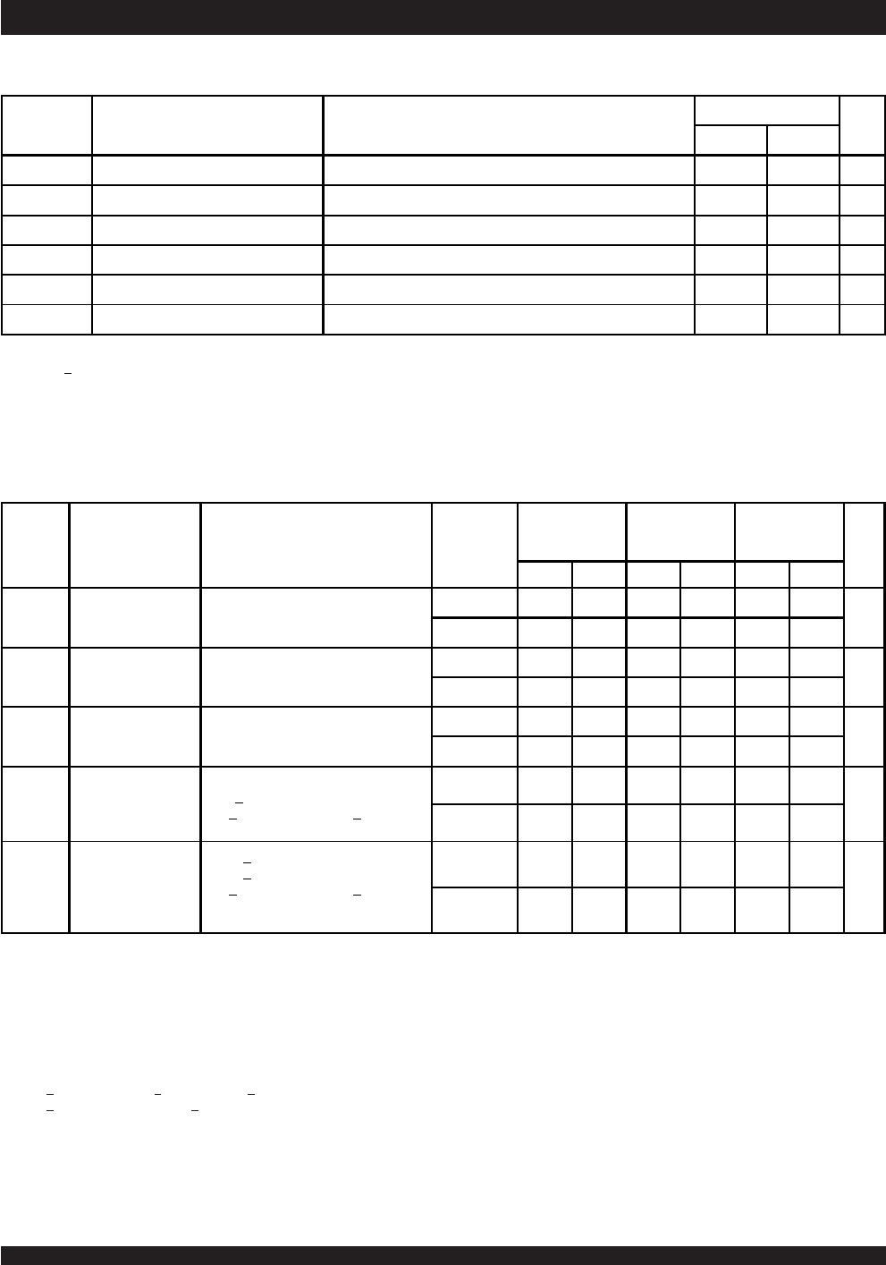
Absolute Maximum Ratings
(1)
NOTES:
1. Stresses greater than those listed under ABSOLUTE MAXIMUM RATINGS
may cause permanent damage to the device. This is a stress rating only
and functional operation of the device at these or any other conditions above
those indicated in the operational sections of this specification is not implied.
Exposure to absolute maximum rating conditions for extended periods may
affect reliability.
2. V
TERM must not exceed VDD + 150mV for more than 25% of the cycle time
or 4ns maximum, and is limited to
< 20mA for the period of VTERM > VDD
+ 150mV.
3. Ambient Temperature under DC Bias. No AC Conditions. Chip Deselected.
Symbol Rating Commercial
& Industrial
Unit
V
TERM
(2)
(V
DD
)
V
DD
Terminal Voltage
with Respect to GND
-0.5 to + 4.6 V
T
BIAS
(3)
Temperature Under Bias -55 to +125
o
C
T
STG
Storage Temperature -65 to +150
o
C
T
JN
Junction Temperature +150
o
C
I
OUT
(For V
DDQ
=
3.3V) DC Output Current 50 mA
I
OUT
(For V
DDQ
=
2.5V) DC Output Current 40 mA
4869 tbl 05
Recommended DC Operating
Conditions with V
DDQ at 3.3V
NOTES:
1. V
IL > -1.5V for pulse width less than 10 ns.
2. V
TERM must not exceed VDDQ + 150mV.
3. To select operation at 3.3V levels on the I/Os and controls of a given port, the
OPT pin for that port must be set to V
DD (3.3V), and VDDQX for that port must be
supplied as indicated above.
Symbol Parameter Min. Typ. Max. Unit
V
DD
Core Supply Voltage 3.15 3.3 3.45 V
V
DDQ
I/O Supply Voltage
(3)
3.15 3.3 3.45 V
V
SS
Ground 0 0 0 V
V
IH
Input High Voltage
(Address & Control Inputs)
(3)
2.0
____
V
DDQ
+ 150mV
(2)
V
V
IH
Input High Voltage - I/O
(3)
2.0
____
V
DDQ
+ 150mV
(2)
V
V
IL
Input Low Voltage -0.3
(1)
____
0.8 V
4869 tbl 07
Recommended DC Operating
Conditions with V
DDQ at 2.5V
NOTES:
1. V
IL > -1.5V for pulse width less than 10 ns.
2. V
TERM must not exceed VDDQ + 100mV.
3. To select operation at 2.5V levels on the I/Os and controls of a given port, the
OPT pin for that port must be set to V
SS (0V), and VDDQX for that port must be
supplied as indicated above.
Symbol Parameter Min. Typ. Max. Unit
V
DD
Core Supply Voltage 3.15 3.3 3.45 V
V
DDQ
I/O Supply Voltage
(3)
2.4 2.5 2.6 V
V
SS
Ground 0 0 0 V
V
IH
Input High Voltage
(3 )
(Address & Control Inputs)
1.7
____
V
DDQ
+ 100mV
(2 )
V
V
IH
Input High Voltage - I/O
(3 )
1.7
____
V
DDQ
+ 100mV
(2 )
V
V
IL
Input Low Voltage -0.5
(1 )
____
0.7 V
4869 tbl 06
Maximum Operating
Temperature and Supply Voltage
(1)
NOTE:
1. This is the parameter TA. This is the "instant on" case temperature.
Grade
Ambient
Temperature GND V
DD
Commercial 0
O
C to +70
O
C0V3.3V
+
150mV
Industrial -40
O
C to +85
O
C0V3.3V
+
150mV
4869 tbl 04
NOTES:
1. These parameters are determined by device characterization, but are not
production tested.
2. C
OUT also references CI/O.
Capacitance
(1)
(TA = +25°C, F = 1.0MHZ) PQFP ONLY
Symbol Parameter Conditions Max. Unit
C
IN
Input Capacitance V
IN
= 0V 8 pF
C
OUT
(2)
Output Capacitance V
OUT
= 0V 10.5 pF
4869 tbl 08