IDT70V659/58/57S
High-Speed 3.3V 128/64/32K x 36 Asynchronous Dual-Port Static RAM Industrial and Commercial Temperature Ranges
6
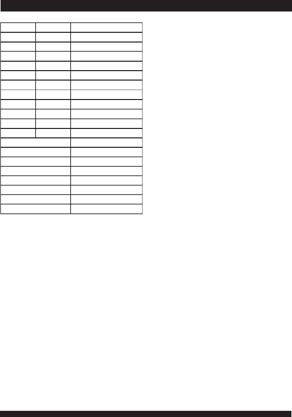
Pin Names
NOTES:
1. V
DD, OPTX, and VDDQX must be set to appropriate operating levels prior to
applying inputs on I/O
X.
2. OPT
X selects the operating voltage levels for the I/Os and controls on that port.
If OPT
X is set to VIH (3.3V), then that port's I/Os and controls will operate at 3.3V
levels and V
DDQX must be supplied at 3.3V. If OPTX is set to VIL (0V), then that
port's I/Os and controls will operate at 2.5V levels and V
DDQX must be supplied
at 2.5V. The OPT pins are independent of one another—both ports can operate
at 3.3V levels, both can operate at 2.5V levels, or either can operate at 3.3V
with the other at 2.5V.
3. Addresses A
16x is a NC for IDT70V658. Also, Addresses A16x and A15x are
NC's for IDT70V657.
4. BUSY is an input as a slave (M/S = V
IL).
Left Port Right Port Names
CE
0L
,
CE
1L
CE
0R
,
CE
1R
Chip Enables - (Input)
R/W
L
R/W
R
Read/Write Enable - (Input)
OE
L
OE
R
Output Enable - (Input)
A
0L
- A
16L
(3)
A
0R
- A
16R
(3)
Address - (Input)
I/O
0L
- I/O
35L
I/O
0R
- I/O
35R
Data Input/Output
SEM
L
SEM
R
Semaphore Enable - (Input)
INT
L
INT
R
Interrupt Flag - (Output)
BUSY
L
BUSY
R
Busy Flag - (Output)
(4)
BE
0L
- BE
3L
BE
0R
- BE
3R
Byte Enables (9-bit bytes) - (Input)
V
DDQL
V
DDQR
Power (I/O Bus) (3.3V or 2.5V)
- (Input)
(1)
OPT
L
OPT
R
Option for selecting V
DDQX
- (Input)
(1,2)
M/S Master or Slave Select - (Input)
V
DD
Power (3.3V) - (Input)
(1)
V
SS
Ground (0V) - (Input)
TDI Test Data Input
TDO Test Data Output
TCK Test Logic Clock (10MHz)
TMS Test Mode Select
TRST
Reset (Initialize TAP Controller)
4869 tbl 01