23
LTC1562
1562fa
R-C Universal Notches
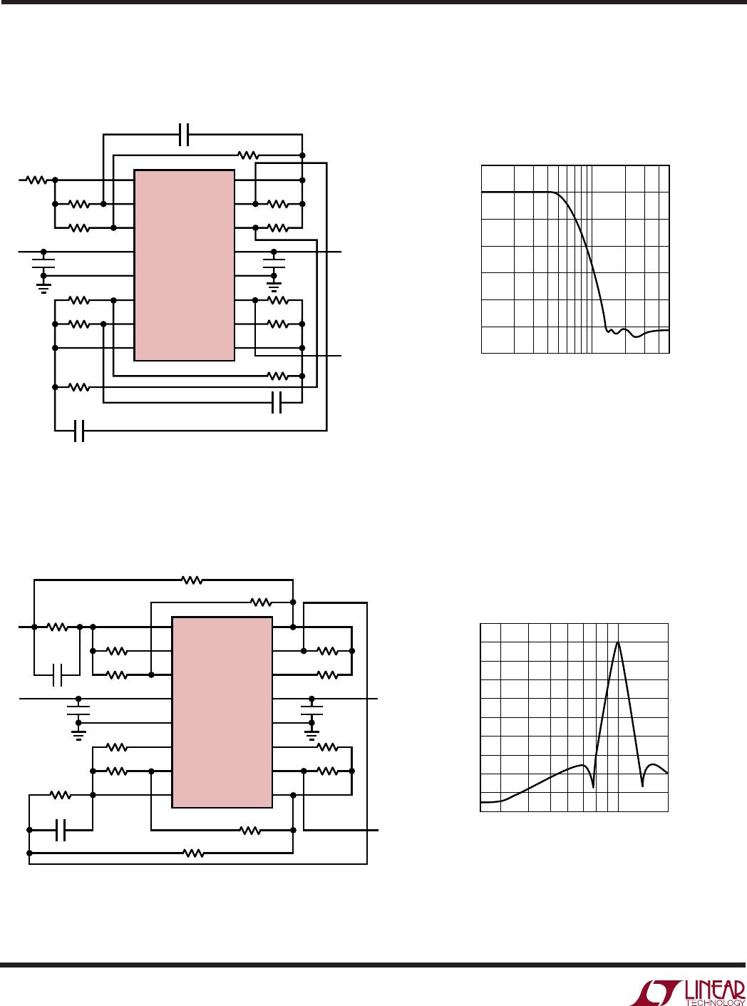
A different way to get 180° phase shift for a notch is to use
the built-in 90° phase difference between the two Opera-
tional Filter block outputs along with a further 90° from an
external capacitor. This method achieves deep notches
independent of component matching, unlike the previous
techniques, and it is convenient for cascaded highpass as
well as lowpass and bandpass filters.
The V2 output of an Operational Filter block is a time-
integrated version of V1 (see Figure 3), and therefore lags
V1 by 90° over a wide range of frequencies. In Figure 16,
a notch response occurs when a 2nd order section drives
a virtual-ground input through two paths, one through a
capacitor and one through a resistor. Again, the virtual
ground may come from an op amp as shown, or from
another Operational Filter block’s INV input. Capacitor C
N
adds a further 90° to the 90° difference between V1 and
V2, producing a wideband 180° phase difference, but
frequency-dependent amplitude ratio, between currents
I
R
and I
C
. At the frequency where I
R
and I
C
have equal
magnitude, I
O
becomes zero and a notch occurs. This
gives a net transfer function from V
IN
to V
OUT
in the form
of H
BR
(s) as above, with parameters:
ƒ=
π
=
N
NN
N
GAIN
IN
N
RCRC
H
R
R
C
C
1
21
1
–
APPLICATIONS INFORMATION
WUU
U
DCGain
R
R
R
R
High Frequency Gain
DCGain
RC
RC
GAIN
IN N
O
N
NN
=
ƒ
ƒ
==
1
2
2
21
21
R1 and C are the internal precision components (in the
LTC1562, 10k and 159pF respectively) as described above
in Setting f
0
and Q.
Unlike the notch methods of Figures 11 and 14, notch
depth from Figure 16 is inherent, not derived from compo-
nent matching. Errors in the R
N
or C
N
values alter the notch
frequency, f
N
, rather than the degree of cancellation at f
N
.
Also, the notch frequency, f
N
, is independent of the section’s
center frequency f
0
, so f
N
can freely be equal to, higher
than or lower than f
0
(Figures 12, 13 or 15, respectively)
without changing the configuration. The chief drawback of
Figure 16 compared to the previous methods is a very
practical one—the C
N
capacitor value directly scales H
N
(and therefore the high frequency gain). Capacitor values
are generally not available in increments or tolerances as
fine as those of resistors, and this configuration lacks the
property of the previous two configurations that sensitiv-
ity to the capacitor value falls as f
N
approaches f
0
. Unlike
the previous notch circuits, this one is also noninverting at
DC.
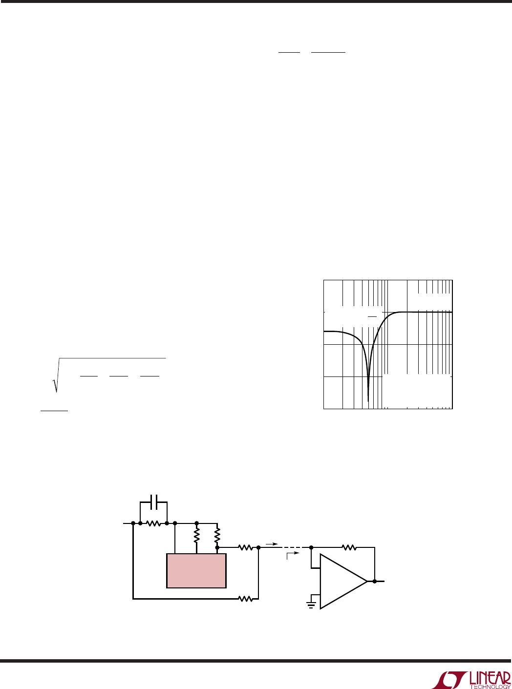
Figure 16. The R-C Universal Notch Configuration for an Operational Filter Block
INV V1
2nd ORDER
1/4 LTC1562
V2
R21
R
Q1
R
IN1
R
N
R
GAIN
I
O
C
N
V
IN
V
OUT
1562 F16
VIRTUAL
GROUND
–
+
I
R
I
C