1
Application Note 1522
ISL9104xxxxEVAL1Z, ISL9104AxxxxEVAL1Z
Evaluation Board Application Manual
Description
The ISL9104 evaluation kit provides a test platform for
the ISL9104 4.3MHz low quiescent current, high
efficiency integrated step-down regulator. The ISL9104 is
capable of delivering 500mA output current. For
adjustable output option, the output voltage can be
programmed through the external feedback resistors R1
and R2 on the board (on board the default output voltage
is set to be 1.6V but it can be programmed for the range
of 0.8V to V
IN
). It is also offered in many fixed output
voltage options including 1.2V, 1.5V, 1.8V, 2.0V, 2.5V,
2.8V and 3.3V.
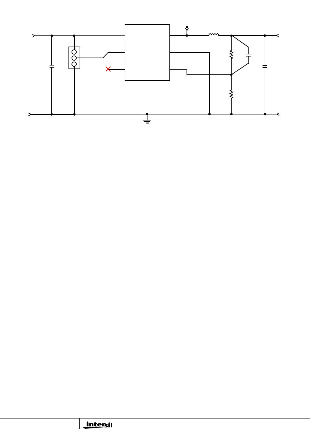
The complete ISL9104 regulator is located at the center
of the board. On the left side of the board are the
connectors for the input power source (VIN and GND).
The output connectors are located on the right side (VO
and GND). Jumper JP1 allows the user to enable or
disable the IC.
The evaluation board schematic, layout and bill of
materials (BOM) can be found at the end of this
application note.
Features
• A Complete Evaluation Platform for ISL9104, ISL9104A
• Convenient Jumpers for Enable/Disable Operation
• Pb-Free (RoHS Compliant)
Recommended Equipment
The following instruments are recommended for testing:
• Power supplies: DC 6.5V/1A
• Electronic load: 0mA to 500mA
• Multimeters
• Function generator
• Oscilloscope
• Cables and wires
Recommended Operating
Conditions
• Input voltage: from 2.7V or (V
OUT
+V
DROP
)
whichever is higher to 6.0V. Here
V
DROP
=I
LOAD
*(r
DSON_PFET
+R
L
). r
DSON_PFET
is
the ON-resistance of the high-side power P-MOSFET
and R
L
is the DCR of the inductor.
• Loading current: 0mA ~ 500mA
• Ambient temperature range: -40
°C ~ +85°C
NOTE: For the fixed output options, the output voltage is
pre-set in the factory. For the adjustable output options, the
output voltage can be programmed through the external
resistor network from VOUT to FB to GND, where
VOUT = 0.8V*(1+R2/R1), please refer to ISL9104, ISL9104A
data sheet FN6829
for recommended component values. On
board, the default output voltage is set at 1.6V for the
adjustable output options.
Setup Guide
1. Place shunt on JP1 at the position of “Enable” to
enable the device. Put shunt on JP1 at the position
of “Disable” will disable the device.
2. Connect the DC power supply between VIN and GND
connectors. Make sure the power supply has enough
supply current capability. Do not adjust the V
IN
higher than the recommended maximum supply
voltage (6.0V).
3. Connect the output to a load (resistor or electronic
load).
4. Turn on the input power supply and evaluate the
device.
Pinout
ISL9104
(6 LD 1.6x1.6 µTDFN)
TOP VIEW
1
3
4
5
6
FB
GND
SW
EN
NC
VIN
2
Ordering Information
PART NUMBER DESCRIPTION
ISL9104IRUNEVAL1Z Evaluation Board for ISL9104IRUNZ-T
(3.3V)
ISL9104IRUJEVAL1Z Evaluation Board for ISL9104IRUJZ-T
(2.8V)
ISL9104IRUFEVAL1Z Evaluation Board for ISL9104IRUFZ-T
(2.5V)
ISL9104IRUDEVAL1Z Evaluation Board for ISL9104IRUDZ-T
(2.0V)
ISL9104IRUCEVAL1Z Evaluation Board for ISL9104IRUCZ-T
(1.8V)
ISL9104IRUBEVAL1Z Evaluation Board for ISL9104IRUBZ-T
(1.5V)
ISL9104IRUWEVAL1Z Evaluation Board for ISL9104IRUWZ-T
(1.2V)
ISL9104IRUAEVAL1Z Evaluation Board for ISL9104IRUAZ-T
(Adjustable)
CAUTION: These devices are sensitive to electrostatic discharge; follow proper IC Handling Procedures.
1-888-INTERSIL or 1-888-468-3774
| Intersil (and design) is a registered trademark of Intersil Americas Inc.
Copyright Intersil Americas Inc. 2010. All Rights Reserved
All other trademarks mentioned are the property of their respective owners.
March 15, 2010
AN1522.1