NB2769ASNR2G

NB2769A
http://onsemi.com
4
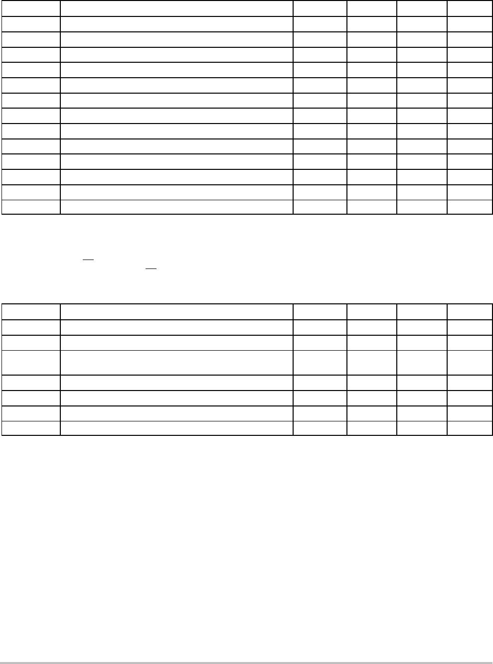
Table 4. DC ELECTRICAL CHARACTERISTICS FOR 2.5 V SUPPLY (Test Conditions: All parameters are measured at room
temperature 25C)
Symbol
Description Min Typ Max Unit
V
IL
Input LOW Voltage GND -- 0.3 0.8 V
V
IH
Input HIGH Voltage 2.0 V
DD
+0.3 V
I
IL
Input LOW Current -- 3 5
mA
I
IH
Input HIGH Current 35
mA
I
XOL
XOUT Output LOW Current (@ 0.5 V, V
DD
=2.5V) 3.0 mA
I
XOH
XOUT Output HIGH Current (@ 1.8 V, V
DD
=2.5V) 3.0 mA
V
OL
Output LOW Voltage (V
DD
=2.5V,I
OL
=8.0mA) 0.6 V
V
OH
Output HIGH Voltage (V
DD
=2.5V,I
OH
=8.0mA) 1.8 V
I
DD
Static Supply Current (Note 1) 10
mA
I
CC
Dynamic Supply Current (2.5 V, 10 MHz, and No Load) 2.5 mA
V
DD
Operating Voltage 2.375 2.5 2.625 V
t
ON
Powerup Time (first locked cycle after powerup) (Note 2) 5.0 mS
Z
OUT
Clock Output Impedance 50
Ω
NOTE: Device will meet the specifications after thermal equilibrium has been established when mounted in a test socket or printed circuit
board with maintained transverse airflow greater than 500 lfpm. Electrical parameters are guaranteed only over the declared
operating temperature range. Functional operation of the device exceeding these conditions is not implied. Device specification limit
values are applied individually under normal operating conditions and not valid simultaneously.
1. XIN/CLKIN pin and PD
are pulled low.
2. V
DD
and XIN/CLKIN input are stable, PD pin is made high from low.
Table 5. AC ELECTRICAL CHARACTERISTICS FOR 2.5 V SUPPLY
Symbol Description Min Typ Max Unit
CLKIN Input Frequency 6.0 12 MHz
ModOUT Output Frequency 6.0 12 MHz
f
d
Frequency Deviation Input Frequency = 6.0 MHz
Input Frequency = 12 MHz
1.51
0.78
%
t
LH
(Note 3) Output Rise Time (measured at 0.7 V to 1.7 V) 0.6 1.2 1.5 ns
t
HL
(Note 3) Output Fall Time (measured at 1.7 V to 0.7 V) 0.4 0.9 1.1 ns
t
JC
Jitter (Cycle--to--Cycle) 200 ps
t
D
Output Duty Cycle 45 50 55 %
NOTE: Device will meet the specifications after thermal equilibrium has been established when mounted in a test socket or printed circuit
board with maintained transverse airflow greater than 500 lfpm. Electrical parameters are guaranteed only over the declared
operating temperature range. Functional operation of the device exceeding these conditions is not implied. Device specification limit
values are applied individually under normal operating conditions and not valid simultaneously.
3. t
LH
and t
HL
are measured at capacitive load of 15 pF.
NB2769A
http://onsemi.com
5
Table 6. DC ELECTRICAL CHARACTERISTICS FOR 3.3 V SUPPLY (Test Conditions: All parameters are measured at room
temperature 25C)
Symbol
Description Min Typ Max Unit
V
IL
Input LOW Voltage GND -- 0.3 0.8 V
V
IH
Input HIGH Voltage 2.0 V
DD
+0.3 V
I
IL
Input LOW Current -- 3 5
mA
I
IH
Input HIGH Current 35
mA
I
XOL
XOUT Output LOW Current (@ 0.4 V, V
DD
=3.3V) 3.0 mA
I
XOH
XOUT Output HIGH Current (@ 2.5 V, V
DD
=3.3V) 3.0 mA
V
OL
Output LOW Voltage (V
DD
=3.3V,I
OL
=8.0mA) 0.4 V
V
OH
Output HIGH Voltage (V
DD
=3.3V,I
OH
=8.0mA) 2.5 V
I
DD
Static Supply Current (Note 4) 10
mA
I
CC
Dynamic Supply Current (3.3 V, 10 MHz, and No Load) 3.5 mA
V
DD
Operating Voltage 2.7 3.3 3.6 V
t
ON
Powerup Time (first locked cycle after powerup) (Note 5) 5.0 mS
Z
OUT
Clock Output Impedance 45
Ω
NOTE: Device will meet the specifications after thermal equilibrium has been established when mounted in a test socket or printed circuit
board with maintained transverse airflow greater than 500 lfpm. Electrical parameters are guaranteed only over the declared
operating temperature range. Functional operation of the device exceeding these conditions is not implied. Device specification limit
values are applied individually under normal operating conditions and not valid simultaneously.
4. XIN/CLKIN pin and PD
are pulled low.
5. V
DD
and XIN/CLKIN input are stable, PD pin is made high from low.
Table 7. AC ELECTRICAL CHARACTERISTICS FOR 3.3 V SUPPLY
Symbol Description Min Typ Max Unit
CLKIN Input Frequency 6.0 13 MHz
ModOUT Output Frequency 6.0 13 MHz
f
d
Frequency Deviation Input Frequency = 6.0 MHz
Input Frequency = 13 MHz
1.51
0.75
%
t
LH
(Note 6) Output Rise Time (measured at 0.8 V to 2.0 V) 0.4 1.2 1.4 ns
t
HL
(Note 6) Output Fall Time (measured at 2.0 V to 0.8 V) 0.3 0.9 1.1 ns
t
JC
Jitter (Cycle--to--Cycle) 200 ps
t
D
Output Duty Cycle 45 50 55 %
NOTE: Device will meet the specifications after thermal equilibrium has been established when mounted in a test socket or printed circuit
board with maintained transverse airflow greater than 500 lfpm. Electrical parameters are guaranteed only over the declared
operating temperature range. Functional operation of the device exceeding these conditions is not implied. Device specification limit
values are applied individually under normal operating conditions and not valid simultaneously.
6. t
LH
and t
HL
are measured at capacitive load of 15 pF.
NB2769A
http://onsemi.com
6
Figure 4. Typical Crystal Oscillator Circuit
Crystal
C1=27pF C2=27pF
R1 = 510 Ω
XIN XOUT
Table 8. TYPICAL CRYSTAL SPECIFICATIONS
Fundamental AT Cut Parallel Resonant Crystal
Nominal Frequency 8.0 MHz
Frequency Tolerance 50 ppm or better at 25C
Operating Temperature Range -- 2 5 Cto+85C
Storage Temperature -- 4 0 Cto+85C
Load Capacitance 18 pF
Shunt Capacitance 7 pF Maximum
ESR
25 Ω

NB2769ASNR2G

Mfr. #:
Manufacturer:
ON Semiconductor
Description:
Phase Locked Loops - PLL HF - EMI REDUCER
Lifecycle:
New from this manufacturer.
Delivery:
DHL FedEx Ups TNT EMS
Payment:
T/T Paypal Visa MoneyGram Western Union

Products related to this Datasheet