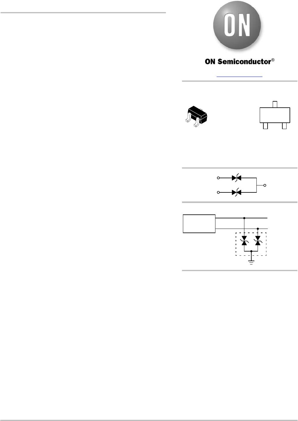
NUP2125, SZNUP2125
www.onsemi.com
2
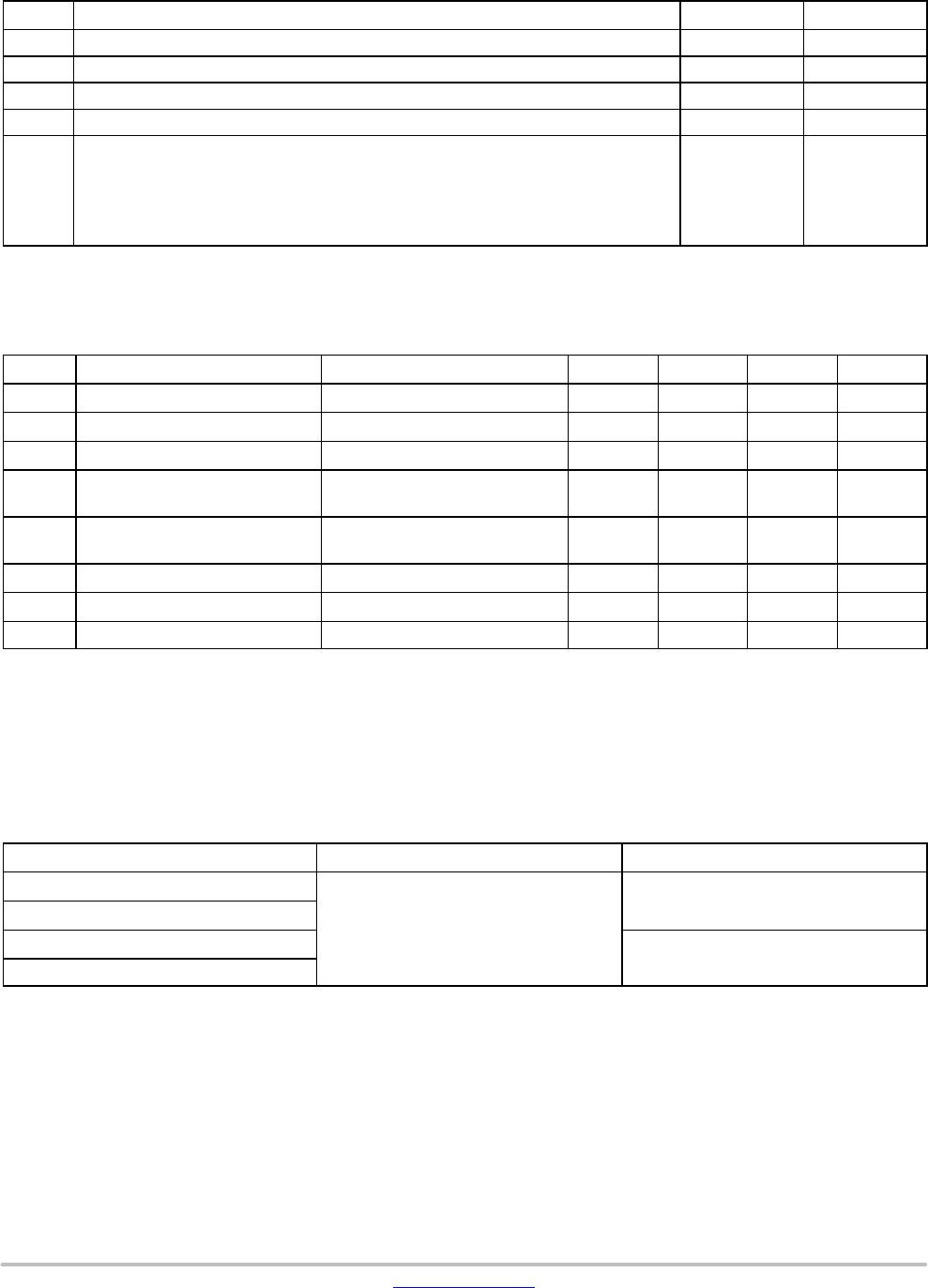
MAXIMUM RATINGS (T
J
= 25°C, unless otherwise specified)
Symbol
Rating Value Unit
PPK
Peak Power Dissipation, 8 x 20 ms Double Exponential Waveform (Note 1)
200 W
T
J
Operating Junction Temperature Range −55 to 150 °C
T
J
Storage Temperature Range −55 to 150 °C
T
L
Lead Solder Temperature (10 s) 260 °C
ESD Human Body Model (HBM)
Machine Model (MM)
IEC 61000−4−2 Contact
IEC 61000−4−2 Air
ISO 10605 150 pF / 2 kW Contact
ISO 10605 330 pF / 2 kW Contact
8.0
1.6
30
30
30
30
kV
kV
kV
kV
kV
kV
Stresses exceeding those listed in the Maximum Ratings table may damage the device. If any of these limits are exceeded, device functionality
should not be assumed, damage may occur and reliability may be affected.
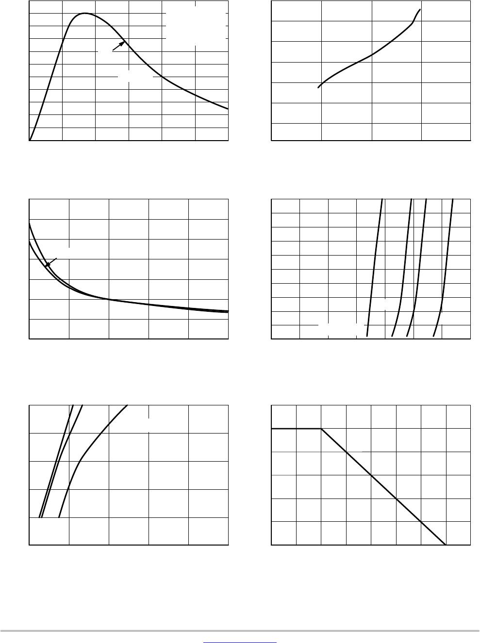
1. Non−repetitive current pulse per Figure 1.
ELECTRICAL CHARACTERISTICS (T
J
= 25°C, unless otherwise specified)
Symbol
Parameter Test Conditions Min Typ Max Unit
V
RWM
Reverse Working Voltage (Note 2) 24 − − V
V
BR
Breakdown Voltage I
T
= 1 mA (Note 3) 26.2 28.5 32 V
I
R
Reverse Leakage Current V
RWM
= 24 V − 15 100 nA
V
C
Clamping Voltage
I
PP
= 1 A (8/20 ms Waveform)
(Note 4)
− 33.4 36.6 V
V
C
Clamping Voltage
I
PP
= 3 A (8/20 ms Waveform)
(Note 4)
− 44 50 V
I
PP
Maximum Peak Pulse Current
8/20 ms Waveform (Note 4)
− − 3.0 A
C
J
Capacitance V
R
= 0 V, f = 1 MHz (Line to GND) − − 10 pF
DC
Diode Capacitance Matching V
R
= 0 V, 5 MHz (Note 5) − 0.26 2 %
Product parametric performance is indicated in the Electrical Characteristics for the listed test conditions, unless otherwise noted. Product
performance may not be indicated by the Electrical Characteristics if operated under different conditions.
2. TVS devices are normally selected according to the working peak reverse voltage (V
RWM
), which should be equal or greater than the DC
or continuous peak operating voltage level.
3. V
BR
is measured at pulse test current I
T
.
4. Pulse waveform per Figure 1.
5. DC is the percentage difference between C
J
of lines 1 and 2 measured according to the test conditions given in the electrical characteristics
table.
ORDERING INFORMATION
Device Package Shipping
†
NUP2125WTT1G
SC−70
(Pb−Free)
3000 / Tape & Reel
SZNUP2125WTT1G*
NUP2125WTT3G
10000 / Tape & Reel
SZNUP2125WTT3G*
†For information on tape and reel specifications, including part orientation and tape sizes, please refer to our Tape and Reel Packaging
Specifications Brochure, BRD8011/D.
*SZ Prefix for Automotive and Other Applications Requiring Unique Site and Control Change Requirements; AEC−Q101 Qualified and PPAP
Capable.