© Semiconductor Components Industries, LLC, 2014
June, 2014 − Rev. 3
1 Publication Order Number:
NTD4858N/D
NTD4858N
Power MOSFET
25 V, 73 A, Single N−Channel, DPAK/IPAK
Features
• Trench Technology
• Low R
DS(on)
to Minimize Conduction Losses
• Low Capacitance to Minimize Driver Losses
• Optimized Gate Charge to Minimize Switching Losses
• These are Pb−Free Devices
Applications
• VCORE Applications
• DC−DC Converters
• High/Low Side Switching
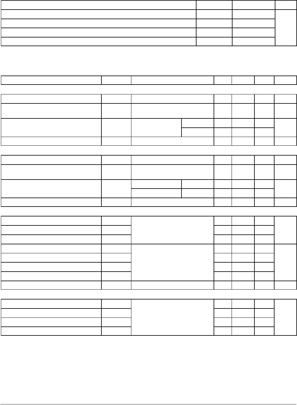
MAXIMUM RATINGS (T
J
= 25°C unless otherwise stated)
Parameter Symbol Value Unit
Drain−to−Source Voltage V
DSS
25 V
Gate−to−Source Voltage V
GS
±20 V
Continuous Drain
Current R
q
JA
(Note 1)
Steady
State
T
A
= 25°C
I
D
14
A
T
A
= 85°C 10.9
Power Dissipation
R
q
JA
(Note 1)
T
A
= 25°C P
D
2.0 W
Continuous Drain
Current R
q
JA
(Note 2)
T
A
= 25°C
ID
11.2
A
T
A
= 85°C 8.7
Power Dissipation
R
q
JA
(Note 2)
T
A
= 25°C P
D
1.3 W
Continuous Drain
Current R
q
JC
(Note 1)
T
C
= 25°C
I
D
73
A
T
C
= 85°C 56
Power Dissipation
R
q
JC
(Note 1)
T
C
= 25°C P
D
54.5 W
Pulsed Drain
Current
t
p
=10ms
T
A
= 25°C I
DM
146 A
Current Limited by Package T
A
= 25°C I
DmaxPkg
45 A
Operating Junction and Storage
Temperature
T
J
,
T
STG
−55 to
+175
°C
Source Current (Body Diode) I
S
45 A
Drain to Source dV/dt dV/dt 6 V/ns
Single Pulse Drain−to−Source Avalanche
Energy (T
J
= 25°C, V
DD
= 50 V, V
GS
= 10 V,
I
L
= 15 A
pk
, L = 1.0 mH, R
G
= 25 W)
EAS 112.5 mJ
Lead Temperature for Soldering Purposes
(1/8” from case for 10 s)
T
L
260 °C
Stresses exceeding those listed in the Maximum Ratings table may damage the
device. If any of these limits are exceeded, device functionality should not be
assumed, damage may occur and reliability may be affected.
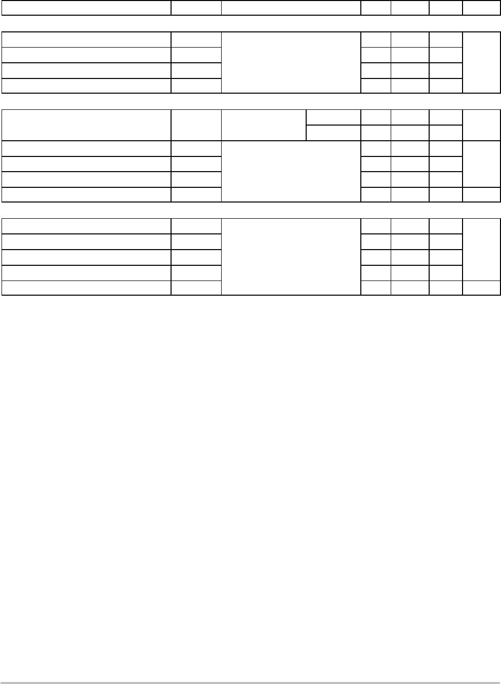
MARKING DIAGRAMS
& PIN ASSIGNMENTS
http://onsemi.com
V
(BR)DSS
R
DS(ON)
MAX I
D
MAX
25 V
6.2 mW @ 10 V
73 A
9.3 mW @ 4.5 V
G
S
N−CHANNEL MOSFET
D
See detailed ordering and shipping information in the package
dimensions section on page 6 of this data sheet.
ORDERING INFORMATION
AYWW
48
58NG
1
Gate
2
Drain
3
Source
4
Drain
4
Drain
2
Drain
1
Gate
3
Sourc
4
Drain
2
Drain
1
Gate
3
Source
AYWW
48
58NG
AYWW
48
58NG
A = Assembly Location*
Y = Year
WW = Work Week
4858N = Device Code
G = Pb−Free Package
DPAK
CASE 369AA
(Bent Lead)
STYLE 2
IPAK
CASE 369D
(Straight Lead
DPAK) STYLE
1
2
3
4
1
2
3
4
IPAK
CASE 369AD
(Straight Lead)
STYLE 2
1
2
3
4
* The Assembly Location code (A) is front side
optional. In cases where the Assembly Location is
stamped in the package, the front side assembly
code may be blank.