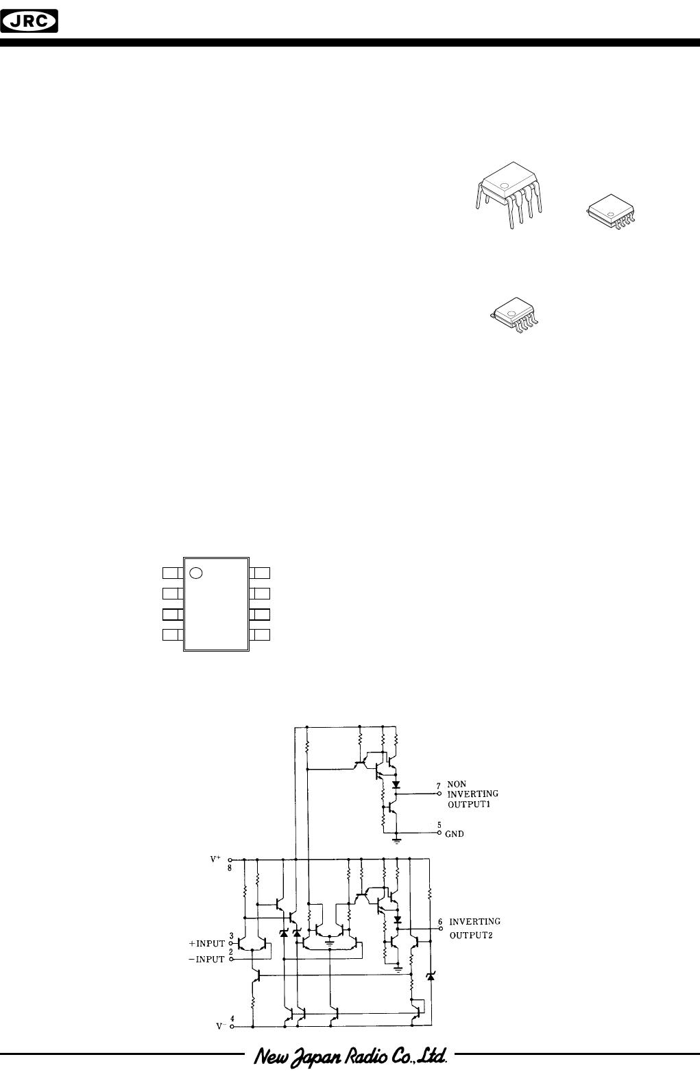
NJM360
-
-
Ver.2011-12-12
■ ABSOLUTE MAXIMUM RATINGS
( Ta=25˚C )
PARAMETER SYMBOL RATINGS UNIT
Supply Voltage V
+
/V
-
± 8 V
Differential Input Voltage V
ID
± 5 V
Input Voltage V
I
± 8 ( note1 ) V
( DIP8 ) 500
( DMP8 ) 300
Power Dissipation P
D
( SOP8 ) 300
mW
Maximum Output Current I
O
± 20 mA
Operating Temperature Range T
opr
-40~+85 ˚C
Storage Temperature Range T
stg
-40~+125 ˚C
( note1 ) For supply voltage less than ±8V,the absolute input voltage is equal to the supply voltage.
■ ELECTRICAL CHARACTERISTICS
( Ta=25˚C
)
PARAMETER SYMBOL TEST CONDITION MIN. TYP. MAX. UNIT
Operating Supply Voltage V
+
4.5 5 6.5 V
Operating Supply Voltage V
-
-4.5 -5 -6.5 V
Input Offset Voltage V
IO
R
S
≤200Ω
- 2 5 mV
Input Offset Current I
IO
- 0.5 3 μA
Input Bias Current I
B
- 5 20 μA
Output Resistance R
O
V
OUT
=V
OM
- 100 - Ω
Response Time 1 t
R1
V
+
/V
-
=± 5V ( note1 ) - 13 25 ns
Response Time 2 t
R2
V
+
/V
-
=± 5V ( note2 ) - 12 20 ns
Response Time 3 t
R3
V
+
/V
-
=± 5V ( note3 ) - 14 - ns
Response Time Difference Between Outputs
( t
pd
of+V
IN1
)-( t
pd
of-V
IN2
) ( note1 ) - 2 - ns
( t
pd
of+V
IN2
)-( t
pd
of-V
IN1
) ( note1 ) - 2 - ns
( t
pd
of+V
IN1
)-( t
pd
of+V
IN2
) ( note1 ) - 2 - ns
( t
pd
of-V
IN1
)-( t
pd
of-V
IN2
) ( note1 ) - 2 - ns
Input Resistance R
IN
f=1MHz - 17 - kΩ
Input Capacitance C
IN
f=1MHz - 3 - pF
Average Temperature Coefficient of Input Offset Voltage ΔV
IO
/ΔT R
S
=50Ω - 8 - μV/˚C
Average Temperature Coefficient of Input Offset Current ΔI
IO
/ΔT - 7 - nA/˚C
Common Mode Input Voltage Range V
ICM
V
+
/V
-
=± 6.5V ± 4 ± 4.5 - V
Differential Input Voltage Range V
ID
± 5 - - V
Output High Voltage ( High ) V
OH
V
+
/V
-
=± 4.5V,I
OUT
=-320μA2.4 3 - V
Output Low Voltage ( Low ) V
OL
V
+
/V
-
=± 4.5V,I
SINK
=6.4mA - 0.25 0.4 V
Positive Supply Current I
+
V
+
/V
-
=± 6.5V - 18 32 mA
Negative Supply Current I
-
V
+
/V
-
=± 6.5V - -9 -16 mA
( note1 ) Response time measured from the 50% point of a 30mV
P-P
10MHz sinusoidal input to the 50% point of the output.
( note2 ) Response time measured from the 50% point of a 2V
P-P
10MHz sinusoidal input to the 50% point of the output.
( note3 ) Response time measured from the start of a 100mV input step with 5mV overdrive to the time when the output crosses the logic threshold.