General Description
The MAX4983E/MAX4984E are high ESD-protected
analog switches that combine the low on-capacitance
and low on-resistance necessary for high-performance
switching applications. COM1 and COM2 are protected
against ±15kV ESD without latchup or damage. The
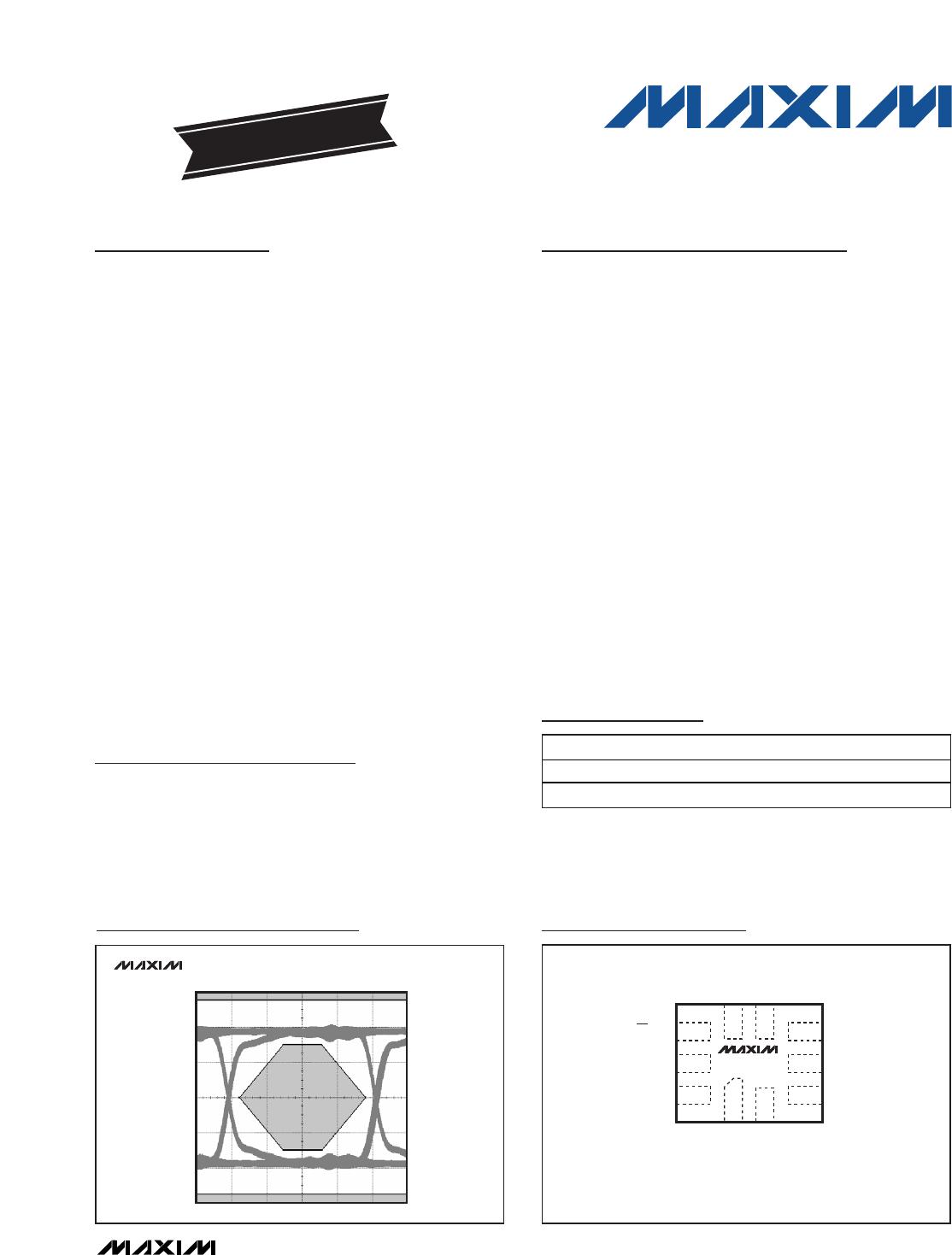
devices are ideal for USB 2.0 Hi-Speed applications at
480Mbps. The switches also handle all the require-
ments for USB low- and full-speed signaling.
The MAX4983E/MAX4984E double-pole/double-throw
(DPDT) switches are fully specified to operate from a
single +2.8V to +5.5V power supply and are protected
against a +5.5V short to COM1 and COM2. This feature
makes the MAX4983E/MAX4984E fully compliant with
the USB 2.0 specification of VBUS fault protection. The
devices feature low-threshold-voltage logic inputs, per-
mitting them to be used with low I/O voltage systems.
The MAX4983E features an active-low enable input
(EN) that when driven high sets the device in shutdown
mode. The MAX4984E features an active-high enable
input (EN) that when driven low sets the device in shut-
down mode. When the device is in shutdown mode, the
quiescent supply current is reduced to 0.1µA.
The MAX4983E/MAX4984E are available in a space-
saving, 10-pin, 1.4mm x 1.8mm UTQFN package, and
operate over a -40°C to +85°C temperature range.
Applications
Features
♦ USB Hi-Speed Switching
♦ ESD Protection on COM
±15kV Human Body Model
±15kV IEC 61000-4-2 Air Gap
±8kV IEC 61000-4-2 Contact
♦ Power-Supply Range: +2.8V to +5.5V
♦ Low 5Ω (typ) On-Resistance (R
ON
)
♦ -3dB Bandwidth: 950MHz (typ)
♦ Compatible with Logic I/O Down to 1.4V
♦ COM Analog Inputs Fault Protected Against
Shorts to +5.5V
♦ Low Supply Current 0.6µA (typ)
♦ Enable Input:
Active-Low (EN) MAX4983E
Active-High (EN) MAX4984E
♦ Small 10-Pin, 1.4mm x 1.8mm UTQFN
MAX4983E/MAX4984E
Hi-Speed USB 2.0 Switches
with ±15kV ESD
________________________________________________________________
Maxim Integrated Products
1
19-4035; Rev 2; 9/08
For pricing, delivery, and ordering information, please contact Maxim Direct at 1-888-629-4642,
or visit Maxim’s website at www.maxim-ic.com.
EVALUATION KIT
AVAILABLE
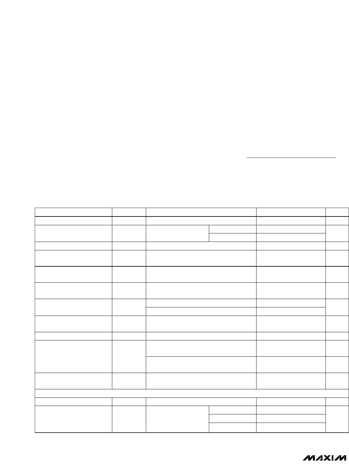
Pin Configuration
(EN) FOR MAX4984E ONLY.