ADF4106 Data Sheet
ABSOLUTE MAXIMUM RATINGS
T
A
= 25°C, unless otherwise noted.
Table 3.
Parameter Rating
AV
DD
to GND
1
0.3 V to + 3.6 V
AV
DD
to DV
DD
0.3 V to + 0.3 V
V
P
to GND 0.3 V to + 5.8 V
V
P
to AV
DD
0.3 V to + 5.8 V
Digital I/O Voltage to GND 0.3 V to V
DD
+ 0.3 V
Analog I/O Voltage to GND 0.3 V to V
P
+ 0.3 V
REF
IN
, RF
IN
A, RF
IN
B to GND
0.3 V to V
DD
+ 0.3 V
RF
IN
A to RF
IN
B ±600 mV
Operating Temperature Range
Industrial (B Version) 40°C to +85°C
Storage Temperature Range 65°C to +125°C
Maximum Junction Temperature 150°C
TSSOP θ
JA
Thermal Impedance
112°C/W
LFCSP θ
JA
Thermal Impedance
(Paddle Soldered)
30.4°C/W
Reflow Soldering
Peak Temperature 260°C
Time at Peak Temperature 40 sec
Transistor Count
CMOS 6425
Bipolar 303
1
GND = AGND = DGND = 0 V.
Stresses at or above those listed under Absolute Maximum
Ratings may cause permanent damage to the product. This is a
stress rating only; functional operation of the product at these
or any other conditions above those indicated in the operational
section of this specification is not implied. Operation beyond
the maximum operating conditions for extended periods may
affect product reliability.
This device is a high performance RF integrated circuit with an
ESD rating of <2 kV, and it is ESD sensitive. Proper precautions
should be taken for handling and assembly.
ESD CAUTION
Rev. F | Page 6 of 24
Data Sheet ADF4106
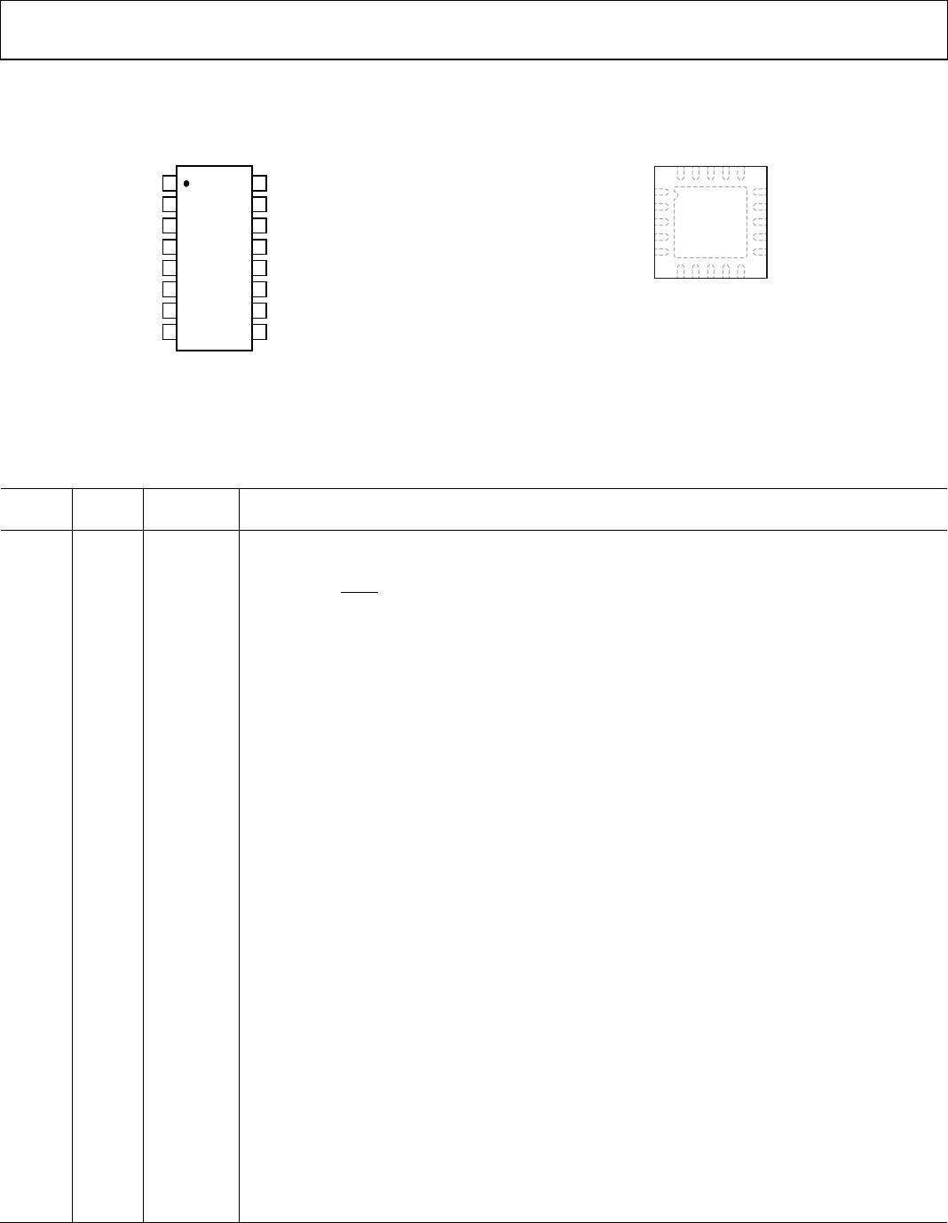
PIN CONFIGURATIONS AND FUNCTION DESCRIPTIONS
02720-003
R
SET
CP
CPGND
AGND
1
2
3
4
5
6
7
8
RF
IN
B
RF
IN
A
AV
DD
REF
IN
MUXOUT
LE
DATA
CLK
CE
DGND
16
15
14
13
12
11
10
9
V
P
DV
DD
TOP VIEW
(Not to Scale)
ADF4106
NOTE: TRANSISTOR COUNT 6425 (CMOS),
303 (BIPOLAR).
Figure 3. 16-Lead TSSOP Pin Configuration
02720-004
14
13
12
1
3
4
LE
15 MUXOUT
DATA
CLK
11
CE
CPGND
AGND
2
AGND
RF
IN
B
5
RF
IN
A
7
AV
DD
6
AV
DD
8
REF
IN
9
DGND
10
DGND
19
R
SET
20
CP
18
V
P
17
DV
DD
16
DV
DD
ADF4106
TOP VIEW
(Not to Scale)
NOTES
1. TRANSISTOR COUNT 6425 (CMOS),
303 (BIPOLAR).
2. THE EXPOSED PAD MUST BE
CONNECTED TO AGND.
Figure 4. 20-Lead LFCSP_WQ Pin Configuration
Table 4. Pin Function Descriptions
Pin No.
TSSOP
Pin No.
LFCSP Mnemonic Function
1 19 R
SET
Connecting a resistor between this pin and CPGND sets the maximum charge pump output current.
The nominal voltage potential at the R
SET
pin is 0.66 V. The relationship between I
CP
and R
SET
is
SET
MAXCP
R
I
5.25
=
So, with R
SET
= 5.1 kΩ, I
CP MAX
= 5 mA.
2 20 CP
Charge Pump Output. When enabled, this provides ±I
CP
to the external loop filter, which in turn
drives the external VCO.
3 1 CPGND Charge Pump Ground. This is the ground return path for the charge pump.
4 2, 3 AGND Analog Ground. This is the ground return path of the prescaler.
5
4
RF
IN
B
Complementary Input to the RF Prescaler. This point must be decoupled to the ground plane with
a small bypass capacitor, typically 100 pF. See Figure 18.
6 5 RF
IN
A Input to the RF Prescaler. This small signal input is ac-coupled to the external VCO.
7 6, 7 AV
DD
Analog Power Supply. This may range from 2.7 V to 3.3 V. Decoupling capacitors to the analog ground
plane should be placed as close as possible to this pin. AV
DD
must be the same value as DV
DD
.
8 8 REF
IN
Reference Input. This is a CMOS input with a nominal threshold of V
DD
/2 and a dc equivalent input
resistance of 100 kΩ. See Figure 18. This input can be driven from a TTL or CMOS crystal oscillator or
it can be ac-coupled.
9 9, 10 DGND Digital Ground.
10 11 CE
Chip Enable. A logic low on this pin powers down the device and puts the charge pump output
into three-state mode. Taking the pin high powers up the device, depending on the status of the
power-down bit, F2.
11 12 CLK
Serial Clock Input. This serial clock is used to clock in the serial data to the registers. The data is latched
into the 24-bit shift register on the CLK rising edge. This input is a high impedance CMOS input.
12 13 DATA
Serial Data Input. The serial data is loaded MSB first with the two LSBs being the control bits.
This input is a high impedance CMOS input.
13 14 LE
Load Enable, CMOS Input. When LE goes high, the data stored in the shift registers is loaded into one
of the four latches with the latch being selected using the control bits.
14 15 MUXOUT
This multiplexer output allows either the lock detect, the scaled RF, or the scaled reference frequency
to be accessed externally.
15 16, 17 DV
DD
Digital Power Supply. This may range from 2.7 V to 3.3 V. Decoupling capacitors to the digital ground
plane should be placed as close as possible to this pin. DV
DD
must be the same value as AV
DD
.
16
18
V
P
Charge Pump Power Supply. This should be greater than or equal to V
DD
. In systems where V
DD
is 3 V,
it can be set to 5.5 V and used to drive a VCO with a tuning range of up to 5 V.
EP Exposed Pad. The exposed pad must be connected to AGND.
Rev. F | Page 7 of 24
ADF4106 Data Sheet
TYPICAL PERFORMANCE CHARACTERISTICS
02720-005
FREQ MAGS11 ANGS11
0.500 0.89148 –17.2820
0.600 0.88133 – 20.6919
0.700
0.87152 – 24.5386
0.800
0.85855
27.3228
0.900 0.84911
–31.0698
1.000 0.83512 – 34.8623
1.100 0.82374 –38.5574
1.200 0.80871 –41.9093
1.300 0.79176 – 45.6990
1.400 0.77205 –49.4185
1.500 0.75696 –52.8898
1.600 0.74234 –56.2923
1.700 0.72239 –60.2584
1.800
0.69419 –63.1446
1.900 0.67288
–65.6464
2.000 0.66227 –68.0742
2.100 0.64758 –71.3530
2.200 0.62454 –75.5658
2.300 0.59466 –79.6404
2.400 0.55932 –82.8246
2.500 0.52256 –85.2795
2.600 0.48754 –85.6298
2.700 0.46411 –86.1854
2.800 0.45776 –86.4997
2.900 0.44859 –88.8080
3.000 0.44588 –91.9737
3.100 0.43810 –95.4087
3.200 0.43269
99.1282
FREQ MAGS11 ANGS11
3.300 0.42777 –102.748
3.400 0.42859 –107.167
3.500 0.43365 –111.883
3.600 0.43849 –117.548
3.700 0.44475 –123.856
3.800
0.44800 –130.399
3.900 0.45223
136.744
4.000 0.45555
142.766
4.100 0.45313 –149.269
4.200 0.45622 –154.884
4.300 0.45555 –159.680
4.400 0.46108 –164.916
4.500 0.45325 –168.452
4.600 0.45054 –173.462
4.700 0.45200 –176.697
4.800 0.45043 178.824
4.900 0.45282 174.947
5.000 0.44287
170.237
5.100 0.44909 166.617
5.200 0.44294 162.786
5.300 0.44558 158.766
5.400 0.45417 153.195
5.500 0.46038 147.721
5.600 0.47128 139.760
5.700 0.47439 132.657
5.800 0.48604 125.782
5.900 0.50637 121.110
6.000 0.52172 115.400
FREQ UNIT GHz KEYWORD R
PARAM TYPE S IMPEDANCE 50
DATA FORMAT MA
Figure 5. S-Parameter Data for the RF Input
0
–30
–5
10
25
–20
15
02720-006
654
32
10
RF INPUT FREQUENCY (GHz)
RF INPUT POWER (dBm)
V
DD
= 3V
V
P
= 3V
T
A
= +85°C
T
A
=
–40°
C
T
A
= +25°
C
Figure 6. Input Sensitivity
0
–100
90
80
–70
–60
–50
–40
–30
–20
–10
02720-007
–2kHz
1kHz 900MHz 1kHz 2kHz
FREQUENCY
OUTPUT POWER (dB)
V
DD
= 3V, V
P
= 5V
I
CP
= 5mA
PFD FREQUENCY = 200kHz
LOOP BANDWIDTH = 20kHz
RES BANDWIDTH = 10Hz
VIDEO BANDWIDTH = 10Hz
SWEEP = 1.9 SECONDS
AVERAGES = 10
–93.0dBc/Hz
REF LEVEL = –14.3dBm
Figure 7. Phase Noise (900 MHz, 200 kHz, and 20 kHz)
–40
–140
–130
–120
–110
–100
–90
–80
–70
–60
–50
02720-008
100Hz 1MHz
FREQUENCY OFFSET FROM 900MHz CARRIER
OUTPUT POWER (dB)
10dB/DIV
R
L
= –40dBc/Hz
RMS NOISE = 0.36°
Figure 8. Integrated Phase Noise (900 MHz, 200 kHz, and 20 kHz)
0
–100
–90
–80
70
60
50
40
–30
–20
–10
02720-009
400kHz –200kHz
900MHz 200kHz 400kHz
FREQUENCY
OUTPUT POWER (dB)
REF LEVEL = –
14.0dBm
V
DD
= 3V, V
P
= 5V
I
CP
= 5mA
PFD FREQUENCY = 200kHz
LOOP BANDWIDTH = 20kHz
RES BANDWIDTH = 1kHz
VIDEO BANDWIDTH = 1kHz
SWEEP = 2.5 SECONDS
AVERAGES = 30
–91.0dBc/Hz
Figure 9. Reference Spurs (900 MHz, 200 kHz, and 20 kHz)
–83.5dBc/Hz
0
–100
–90
–80
–70
–60
–50
–40
–30
–20
–10
02720-010
–2kHz –1kHz 5800MHz 1kHz 2kHz
FREQUENCY
OUTPUT POWER (dB)
REF LEVEL = –10dBm
V
DD
= 3V, V
P
= 5V
I
CP
= 5mA
PFD FREQUENCY = 1MHz
LOOP BANDWIDTH = 100kHz
RES BANDWIDTH = 10Hz
VIDEO BANDWIDTH = 10Hz
SWEEP = 1.9 SECONDS
AVERAGES = 10
Figure 10. Phase Noise (5.8 GHz,1 MHz, and 100 kHz)
Rev. F | Page 8 of 24

ADF4106BRUZ-RL

Mfr. #:
Manufacturer:
Analog Devices Inc.
Description:
Phase Locked Loops - PLL Freq Synthesizer
Lifecycle:
New from this manufacturer.
Delivery:
DHL FedEx Ups TNT EMS
Payment:
T/T Paypal Visa MoneyGram Western Union