LT3585-0/LT3585-1
LT3585-2/LT3585-3
10
3585f
OPERATIO
U
The LT3585 series of parts operate on the edge of dis-
continuous conduction mode. When CHRG/IADJ is driven
higher than 1.1V, the master latch is set. This enables the
part to deliver power to the photofl ash capacitor. When
the power switch, Q1, is turned on, current builds up in
the primary of the transformer. When the desired current
level is reached, the output of comparator A1 goes high,
resetting the switch latch that controls the state of Q1, and
the output of the DCM comparator goes low. Q1 now turns
off and the fl yback waveform on the SW node quickly rises
to a level proportional to V
OUT
. The secondary current fl ows
through high voltage diode(s), D1, and into the photofl ash
capacitor. When the secondary current decays to zero,
the voltage on the SW node collapses. When this voltage
reaches 130mV higher than V
BAT
, the output of A3 goes
high. This sets the switch latch and the power switch, Q1,
turns back on. This cycle repeats until the target V
OUT
level
is reached. When the target V
OUT
is reached, the master
latch resets and the DONE pin goes low.
The input current of an LT3585 series circuit can be
reduced by changing the voltage of the CHRG/IADJ pin.
When this pin is between 1.1V and 1.4V, a time delay is
added between when A3 goes high and the switch latch
is set, see Figure 2. If the part is enabled, and the CHRG/
IADJ pin is fl oated, internal circuitry drives the voltage on
the pin to 1.28V. This allows a single I/O port pin, which
can be three-stated, to enable or disable the part as well
as place the part into the input current reduction mode.
This feature effectively reduces the average input current
into the fl yback transformer. The magnitude of the delay
decreases with increasing V
BAT
. This causes the reduced
average input current to remain relatively fl at with changes
in V
BAT
. When CHRG/IADJ is brought higher than 1.6V,
no delay is added. The CHRG/IADJ pin functionality is
shown in Figure 3.
Both V
BAT
and V
IN
have undervoltage lockout (UVLO). When
one of these pins goes below its UVLO voltage, the DONE
pin goes low. With an insuffi cient bypass capacitor on V
BAT
or V
IN
, the ripple on the pin is likely to activate UVLO and
terminate the charge. The applications circuits in the data
sheet suggest values adequate for most applications.
The LT3585 series also includes an integrated IGBT driver.
There are two output pins, IGBTPU and IGBTPD. The
IGBTPU pin is used to pull the gate of the IGBT up. This
should be done quickly to guarantee proper Xenon lamp
ignition. Tie this pin directly to the gate of the IGBT. The
IGBTPD pin is pinned out separately to allow for greater
exibility in choosing a series resistor between the pin and
the gate of the IGBT. This resistor can be used to slow
down the turn off of the IGBT.
I
PRI
V
SW
TIME
V
SW
TIME
3585 F02
TIME
I
PRI
TIME
Extra Delay Added
(~5.2µs at V
BAT
= 4.2V)
Normal Operation
CHRG/IADJ 1.6V
Reduced Input Current
CHRG/IADJ Three Stated
Fi
gure
3
.
B
as
i
c
O
pera
ti
on
Fi
gure
2
.
N
orma
l
an
d
R
e
d
uce
d
I
npu
t
C
urren
t
W
ave
f
orms
V
OUT
100V/DIV
DONE
2V/DIV
CHRG/IADJ
2V/DIV
LT3585-1
V
BAT
= 3.6V
C
OUT
= 50µF
*MUST TAKE CHRG/IADJ PIN ABOVE 1.1V, THEN FLOAT
1sec/DIV
<0.3V <0.3V <0.3V3V 3V
THREE
STATE*
CHRG/IADJ PIN STATE
3585 F03
LT3585-0/LT3585-1
LT3585-2/LT3585-3
11
3585f
APPLICATIO S I FOR ATIO
WUUU
Choosing the Right Device
(LT3585-0/LT3585-1/LT3585-2/LT3585-3)
The only difference between the four versions of the
LT3585 series is the peak current level. For the fastest
possible charge time, use the LT3585-3. The LT3585-1
has the lowest peak current capability, and is designed
for applications that need a more limited drain on the
batteries. Due to the lower peak current, the LT3585-1
can use a physically smaller transformer. The LT3585-0
and LT3585-2 have a current limit in between that of the
LT3585-1 and the LT3585-3.
Transformer Design
The fl yback transformer is a key element for any LT3585-0/
LT3585-1/LT3585-2/LT3585-3 design. It must be designed
carefully and checked that it does not cause excessive cur-
rent or voltage on any pin of the part. The main parameters
that need to be designed are shown in Table 1. The fi rst
transformer parameter that needs to be set is the turns
ratio, N. The LT3585-0/LT3585-1/LT3585-2/LT3585-3
accomplish output voltage detection by monitoring the
yback waveform on the SW pin. When the SW voltage
reaches 31.5V higher than the V
BAT
voltage, the part halts
power delivery. Thus, the choice of N sets the target output
voltage and changes the amplitude gain of the refl ected
voltage from the output to the SW pin. Choose N according
to the following equation:
N
V
OUT
=
+ 2
31 5.
where V
OUT
is the desired output voltage. The number 2
in the numerator is used to include the forward voltage
drop across the output diode(s). Thus, for a 320V output,
N should be 322/31.5 or 10.2. For a 300V output, choose
N equal to 302/31.5 or 9.6. The next parameter that needs
to be set is the primary inductance, L
PRI
. Choose L
PRI
according to the following formula:
L
V
NI
PRI
OUT
PK
••
200 10
9
where V
OUT
is the desired output voltage. N is the trans-
former turns ratio. I
PK
is 1.4 (LT3585-0), 0.7 (LT3585-1),
1 (LT3585-2) and 2 (LT3585-3). L
PRI
needs to be equal
or larger than this value to ensure that the LT3585 series
has adequate time to respond to the fl yback waveform.
All other parameters need to meet or exceed the recom-
mended limits as shown in Table 1. A particularly important
parameter is the leakage inductance, L
LEAK
. When the
power switch of the LT3585 series turns off, the leakage
inductance on the primary of the transformer causes a
voltage spike to occur on the SW pin. The height of this
spike must not exceed 50V, even though the absolute
maximum rating of the SW pin is 60V. The 60V absolute
maximum rating is a DC blocking voltage specifi cation,
which assumes that the current in the power NPN is zero.
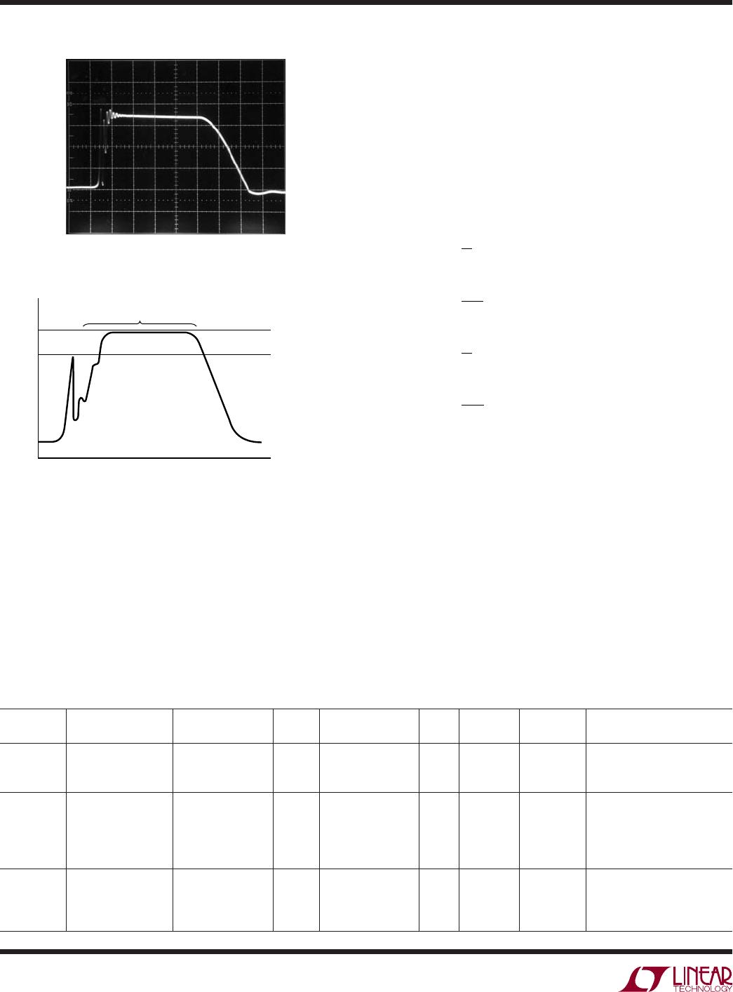
Figure 4 shows the SW voltage waveform for the circuit
of Figure 8 (LT3585-0). Note that the absolute maximum
rating of the SW pin is not exceeded. Make sure to check
the SW voltage waveform with V
OUT
near the target output
voltage, as this is the worst-case condition for SW volt-
age. Figure 5 shows the various limits on the SW voltage
during switch turn off.
Table 1. Recommended Transformer Parameters
PARAMETER NAME
TYPICAL RANGE
LT3585-0
TYPICAL RANGE
LT3585-1
TYPICAL RANGE
LT3585-2
TYPICAL RANGE
LT3585-3 UNITS
L
PRI
Primary Inductance >5 >10 >7 >3.5 µH
L
LEAK
Primary Leakage Inductance 100 to 300 200 to 500 200 to 500 100 to 300 nH
N Secondary/Primary Turns Ratio 8 to 12 8 to 12 8 to 12 8 to 12
V
ISO
Secondary to Primary Isolation
Voltage
>500 >500 >500 >500 V
I
SAT
Primary Saturation Current >1.6 >0.8 >1.0 >2 A
R
PRI
Primary Winding Resistance <300 <500 <400 <200 mΩ
R
SEC
Secondary Winding Resistance <40 <80 <60 <30
Ω
LT3585-0/LT3585-1
LT3585-2/LT3585-3
12
3585f
APPLICATIO S I FOR ATIO
WUUU
It is important not to minimize the leakage inductance to
a very low level. Although this would result in a very low
leakage spike on the SW pin, the parasitic capacitance of the
transformer would become large. This will adversely affect
the charge time of the photofl ash circuit. Linear Technology
has worked with several leading magnetic component man-
ufacturers to produce predesigned fl yback transformers
for use with the LT3585-0 /LT3585-1/LT3585-2/LT3585-3.
Table 2 shows the details of several of these transformers.
Output Diode Selection
The rectifying diode(s) should be low capacitance type
with suffi cient reverse voltage and forward current rat-
ings. The peak reverse voltage that the diode(s) will see
is approximately:
V
PK(R)
= V
OUT
+ (N • V
BAT
)
The peak current of the diode is simply:
I
N
LT
I
N
LT
PK SEC
PK SEC
()
()
.
=
()
=
2
3585 3
14
358
-
55
1
3585 2
07
-0
-
()
=
()
=
I
N
LT
I
N
PK SEC
PK SEC
()
()
.
LT3585 1-
()
For the circuit of Figure 8 with V
BAT
of 5V, V
PK(R)
is 371V
and I
PK(SEC)
is 137mA. The GSD2004S dual silicon diode
is recommended for most applications. Table 3 shows
the various diodes and relevant specifi cations. Use the
appropriate number of diodes to achieve the necessary
reverse breakdown voltage.
Capacitor Selection
For the input bypass capacitors, high quality X5R or X7R
types should be used. Make sure the voltage capability of
the part is adequate.
MUST BE
LESS THAN 60V
MUST BE
LESS THAN 50V
3585 F05
A
B
V
SW
0V
Fi
gure
4
.
LT3585
SW
V
o
lt
age
W
ave
f
orm
Figure 5. New Transformer Design Check
Table 2. Predesigned Transformers—Typical Specifi cations Unless Otherwise Noted
FOR USE
WITH
TRANSFORMER
DESIGNATION
SIZE
(W × L × H) (mm)
LPRI
(µH)
LPRI LEAKAGE
(nH ) N
R
PRI
(mΩ)
R
SEC
(Ω) VENDOR
LT3585-1
LT3585-0/
LT3585-2
SBL-5.6S-1
SBL-5.6-1
5.6 × 8.5 × 3.0
5.6 × 8.5 × 4.0
24
10
400 Max
200 Max
10.2
10.2
305
103
55
26
Kijima Musen
Hong Kong Offi ce
852-2489-8266
LT3585-1
LT3585-0
LT3585-1
LT3585-2
LT3585-3
LDT565620ST-203
LDT565630T-001
LDT565630T-002
LDT565630T-003
LDT565630T-041
5.8 × 5.8 × 2.0
5.8 × 5.8 × 3.0
5.8 × 5.8 × 3.0
5.8 × 5.8 × 3.0
5.8 × 5.8 × 3.0
8.2
6
14.5
10.5
4.7
390 Max
200 Max
500 Max
550 Max
150 Max
10.2
10.4
10.2
10.2
10.4
370 Max
100 Max
240 Max
210 Max
90 Max
11.2 Max
10 Max
16.5 Max
14 Max
6.4 Max
TDK
Chicago Sales Offi ce
(847) 803-6100
www.components.tdk.com
LT3585-0
LT3585-1
LT3585-2
LT3585-3
TTRN-0530-000-T
TTRN-0530-012-T
TTRN-0530-021-T
TTRN-0530-022-T
5.0 × 5.0 × 3.0
5.0 × 5.0 × 3.0
5.0 × 5.0 × 3.0
5.0 × 5.0 × 3.0
6.6
16.0
11.8
4.0
200 Max
400 Max
300 Max
300 Max
10.3
10.3
10.3
10.3
128 Max
515 Max
256 Max
102 Max
28 Max
32 Max
37 Max
16 Max
Tokyo Coil Engineering
Japan Offi ce
0426-56-6262
V
SW
10V/DIV
100ns/DIV
3585 F04
V
BAT
= 3.6V
V
OUT
= 320V

LT3585EDDB-3#TRPBF

Mfr. #:
Manufacturer:
Analog Devices / Linear Technology
Description:
Power Management Specialized - PMIC Photoflash Chr w/ Adj In C & IGBT Drvr
Lifecycle:
New from this manufacturer.
Delivery:
DHL FedEx Ups TNT EMS
Payment:
T/T Paypal Visa MoneyGram Western Union