10CL080YF780C8G

Cyclone 10 LP I/O Vertical Migration
Figure 2. Migration Capability Across Cyclone 10 LP Devices
The arrows indicate the migration paths. The devices included in each vertical
migration path are shaded. Devices with lesser I/O resources in the same path
have lighter shades.
To achieve full I/O migration across devices in the same migration path, restrict
I/O usage to match the device with the lowest I/O count.
Device
Package
M164 U256 U484 E144 F484 F780
10CL006
10CL010
10CL016
10CL025
10CL040
10CL055
10CL080
10CL120
Note: To verify the pin migration compatibility, use the Pin Migration View window in the
Quartus Prime software Pin Planner.
Logic Elements and Logic Array Blocks
The LAB consists of 16 logic elements (LE) and a LAB-wide control block. An LE is the
smallest unit of logic in the Cyclone 10 LP device architecture. Each LE has four inputs,
a four-input look-up table (LUT), a register, and output logic. The four-input LUT is a
function generator that can implement any function with four variables.
Cyclone
®
10 LP Device Overview
Intel
®
Cyclone
®
10 LP Device Overview
7
Figure 3. Cyclone 10 LP Device Family LEs
Row, column, and
direct link routing
data 1
data 2
data 3
data 4
labclr1
labclr2
Chip-wide reset
(DEV_CLRn)
labclk1
labclk2
labclkena1
labclkena2
LE carry-in
LAB-wide
synchronous load
LAB-Wide
synchronous clear
Row, column, and
direct link routing
Local routing
Register chain output
Register bypass
Programmable register
Register chain routing
from previous LE
LE Carry-Out
Register feedback
Synchronous
Load and
Clear Logic
Carry
Chain
Look-Up Table
(LUT)
Asynchronous
Clear Logic
Clock and
Clock Enable
Select
D
Q
ENA
CLRN
Embedded Multipliers
Each embedded multiplier block in Cyclone 10 LP devices supports one individual
18 × 18-bit multiplier or two individual 9 × 9-bit multipliers. You can cascade the
multiplier blocks to form wider or deeper logic structures.
You can control the operation of the embedded multiplier blocks using the following
options:
Parameterize the relevant IP cores with the Quartus Prime parameter editor
Infer the multipliers directly with VHDL or Verilog HDL
Intel and partners offer popular DSP IPs for Cyclone 10 LP devices, including:
Finite impulse response (FIR)
Fast Fourier transform (FFT)
Numerically controlled oscillator (NCO) functions
For a streamlined DSP design flow, the DSP Builder tool integrates the Quartus Prime
software with MathWorks Simulink and MATLAB design environments.
Embedded Memory Blocks
The embedded memory structure consists of M9K memory blocks columns. Each M9K
memory block of a Cyclone 10 LP device provides 9 Kb of on-chip memory. You can
cascade the memory blocks to form wider or deeper logic structures.
You can configure the M9K memory blocks as RAM, FIFO buffers, or ROM.
Cyclone
®
10 LP Device Overview
Intel
®
Cyclone
®
10 LP Device Overview
8
Table 4. M9K Operation Modes and Port Widths
Operation Modes Port Widths
Single port ×1, ×2, ×4, ×8, ×9, ×16, ×18, ×32, and ×36
Simple dual port ×1, ×2, ×4, ×8, ×9, ×16, ×18, ×32, and ×36
True dual port ×1, ×2, ×4, ×8, ×9, ×16, and ×18
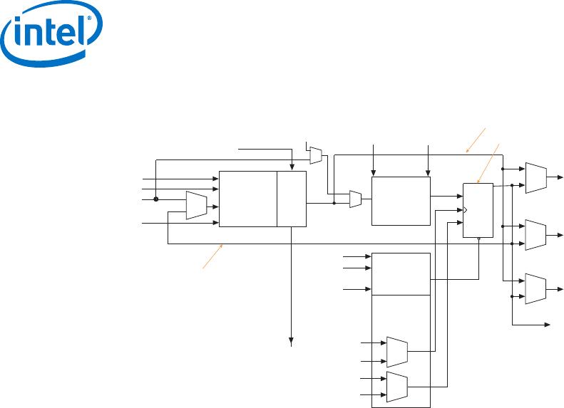
Clocking and PLL
Cyclone 10 LP devices feature global clock (GCLK) networks, dedicated clock pins, and
general purpose PLLs.
Up to 20 GCLK networks that drive throughout the device
Up to 15 dedicated clock pins
Up to four general purpose PLLs with five outputs per PLL
The PLLs provide robust clock management and synthesis for the Cyclone 10 LP
device. You can dynamically reconfigure the PLLs in user mode to change the clock
phase or frequency.
FPGA General Purpose I/O
Cyclone 10 LP devices offer highly configurable GPIOs with these features:
Support for over 20 popular single-ended and differential I/O standards.
Programmable bus hold, pull-up resistors, delay, and drive strength.
Programmable slew-rate control to optimize signal integrity.
Calibrated on-chip series termination (R
S
OCT) or driver impedance matching (R
S
)
for single-endd I/O standards.
True and emulated LVDS buffers with LVDS SERDES implemented using logic
elements in the device core.
Hot socketing support.
Configuration
Cyclone 10 LP devices use SRAM cells to store configuration data. Configuration data
is downloaded to the Cyclone 10 LP device each time the device powers up.
You can use EPCS or EPCQ (AS x1) flash configuration devices to store configuration
data and configure the Cyclone 10 LP FPGAs.
Cyclone 10 LP devices support 1.5 V, 1.8 V, 2.5 V, 3.0 V, and 3.3 V programming
voltages and several configuration schemes.
The single-event upset (SEU) mitigation feature detects cyclic redundancy check
(CRC) errors automatically during configuration and optionally during user mode
1
.
1 User mode error detection is not supported on 1.0 V core voltage Cyclone 10 LP device
variants.
Cyclone
®
10 LP Device Overview
Intel
®
Cyclone
®
10 LP Device Overview
9

10CL080YF780C8G

Mfr. #:
Manufacturer:
Intel / Altera
Description:
FPGA - Field Programmable Gate Array
Lifecycle:
New from this manufacturer.
Delivery:
DHL FedEx Ups TNT EMS
Payment:
T/T Paypal Visa MoneyGram Western Union