6.42
IDT70V05S/L
High-Speed 3.3V 8K x 8 Dual-Port Static RAM Industrial and Commercial Temperature Ranges
8
NOTES:
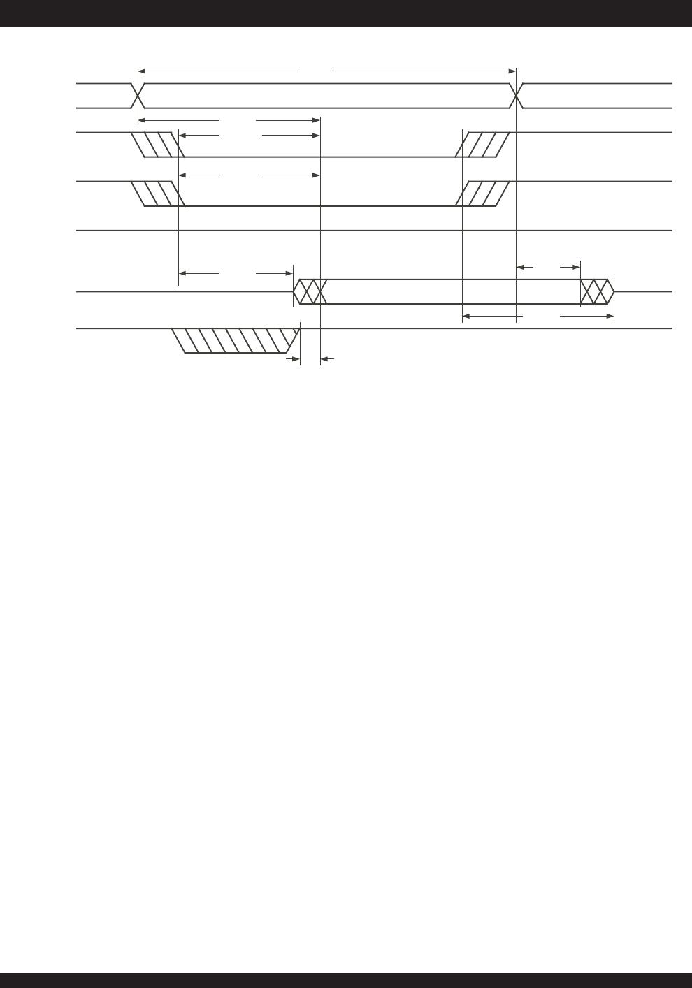
1. Transition is measured 0mV from Low or High-impedance voltage with Output Test Load (Figure 2).
2. This parameter is determined by device characterization but is not production tested.
3. To access SRAM, CE = V
IL, SEM = VIH.
4. 'X' in part number indicates power rating (S or L).
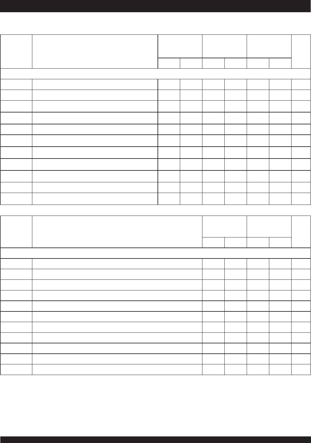
AC Electrical Characteristics Over the
Operating Temperature and Supply Voltage Range
(4)
51X50V07
ylnOl'moC
02X50V07
l'moC
dnI&
52X50V07
ylnOl'moC
tinUlobmySretemaraP.niM.xaM.niM.xaM.niM.xaM
ELCYCDAER
t
CR
emiTelcyCdaeR51
____
02
____
52
____
sn
t
AA
emiTsseccAsserddA
____
51
____
02
____
52sn
t
ECA
emiTsseccAelbanEpihC
)3(
____
51
____
02
____
52sn
t
EOA
emiTsseccAelbanEtuptuO
)3(
____
01
____
21
____
31sn
t
HO
egnahCsserddAmorfdloHtuptuO3
____
3
____
3
____
sn
t
ZL
emiTZ-woLtuptuO
)2,1(
3
____
3
____
3
____
sn
t
ZH
emiTZ-hgiHtuptuO
)2,1(
____
01
____
21
____
51sn
t
UP
emiTpUrewoPotelbanEpihC
)2,1(
0
____
0
____
0
____
sn
t
DP
emiTnwoDrewoPotelbasiDpihC
)2,1(
____
51
____
02
____
52sn
t
POS
(esluPetadpUgalFerohpameS EO ro MES )01
____
01
____
01
____
sn
t
AAS
sseccAsserddAerohpameS
)3(
____
51
____
02
____
52sn
a11lbt1492
53X50V07
ylnOl'moC
55X50V07
ylnOl'moC
tinUlobmySretemaraP.niM.xaM.niM.xaM
ELCYCDAER
t
CR
emiTelcyCdaeR 53
____
55
____
sn
t
AA
emiTsseccAsserddA
____
53
____
55sn
t
ECA
emiTsseccAelbanEpihC
)3(
____
53
____
55sn
t
EOA
emiTsseccAelbanEtuptuO
)3(
____
02
____
03sn
t
HO
egnahCsserddAmorfdloHtuptuO 3
____
3
____
sn
t
ZL
emiTZ-woLtuptuO
)2,1(
3
____
3
____
sn
t
ZH
emiTZ-hgiHtuptuO
)2,1(
____
51
____
52sn
t
UP
emiTpUrewoPotelbanEpihC
)2,1(
0
____
0
____
sn
t
DP
emiTnwoDrewoPotelbasiDpihC
)2,1(
____
53
____
05sn
t
POS
(esluPetadpUgalFerohpameS EO ro MES )51
____
51
____
sn
t
AAS
sseccAsserddAerohpameS
)3(
____
53
____
55sn
b11lbt1492