6.42
IDT70V05S/L
High-Speed 3.3V 8K x 8 Dual-Port Static RAM Industrial and Commercial Temperature Ranges
19
Functional Description
The IDT70V05 provides two ports with separate control, address
and I/O pins that permit independent access for reads or writes to any
location in memory. The IDT70V05 has an automatic power down
feature controlled by CE. The CE controls on-chip power down circuitry
that permits the respective port to go into a standby mode when not
selected (CE HIGH). When a port is enabled, access to the entire
memory array is permitted.
Interrupts
If the user chooses the interrupt function, a memory location (mail
box or message center) is assigned to each port. The left port interrupt
flag (INTL) is set when the right port writes to memory location 1FFE
(HEX). The left port clears the interrupt by reading address location
1FFE. Likewise, the right port interrupt flag (INTR) is set when the left
port writes to memory location 1FFF (HEX) and to clear the interrupt
flag (INTR), the right port must read the memory location 1FFF. The
message (8 bits) at 1FFE or 1FFF is user-defined. If the interrupt
function is not used, address locations 1FFE and 1FFF are not used
as mail boxes, but as part of the random access memory. Refer to
Truth Table III for the interrupt operation.
Busy Logic
Busy Logic provides a hardware indication that both ports of the
SRAM have accessed the same location at the same time. It also
allows one of the two accesses to proceed and signals the other side
that the SRAM is “busy”. The BUSY pin can then be used to stall the
access until the operation on the other side is completed. If a write
operation has been attempted from the side that receives a BUSY
indication, the write signal is gated internally to prevent the write from
proceeding.
The use of BUSY logic is not required or desirable for all applica-
tions. In some cases it may be useful to logically OR the BUSY outputs
together and use any BUSY indication as an interrupt source to flag the
event of an illegal or illogical operation. If the write inhibit function of
BUSY logic is not desirable, the BUSY logic can be disabled by placing
the part in slave mode with the M/S pin. Once in slave mode the BUSY
pin operates solely as a write inhibit input pin. Normal operation can be
programmed by tying the BUSY pins HIGH. If desired, unintended
write operations can be prevented to a port by tying the BUSY pin for
that port LOW.
The BUSY outputs on the IDT 70V05 SRAM in master mode, are
push-pull type outputs and do not require pull up resistors to
operate. If these SRAMs are being expanded in depth, then the
BUSY indication for the resulting array requires the use of an external
AND gate.
Width Expansion with Busy Logic
Master/Slave Arrays
When expanding an IDT70V05 SRAM array in width while using
BUSY logic, one master part is used to decide which side of the RAM
array will receive a BUSY indication, and to output that indication. Any
number of slaves to be addressed in the same address range as the
master, use the BUSY signal as a write inhibit signal. Thus on the
IDT70V05 SRAM the BUSY pin is an output if the part is used as a
master (M/S pin = VIH), and the BUSY pin is an input if the part used
as a slave (M/S pin = VIL) as shown in Figure 3.
If two or more master parts were used when expanding in width, a
split decision could result with one master indicating BUSY on one side
of the array and another master indicating BUSY on one other side of
the array. This would inhibit the write operations from one port for part
of a word and inhibit the write operations from the other port for the
other part of the word.
The BUSY arbitration, on a master, is based on the chip enable and
address signals only. It ignores whether an access is a read or write.
In a master/slave array, both address and chip enable must be valid
long enough for a BUSY flag to be output from the master before the
actual write pulse can be initiated with the R/W signal. Failure to
observe this timing can result in a glitched internal write inhibit signal
and corrupted data in the slave.
Semaphores
The IDT70V05 is a fast Dual-Port 8K x 8 CMOS Static RAM with
an additional 8 address locations dedicated to binary semaphore flags.
These flags allow either processor on the left or right side of the Dual-
Port SRAM to claim a privilege over the other processor for functions
defined by the system designer’s software. As an example, the
semaphore can be used by one processor to inhibit the other from
accessing a portion of the Dual-Port SRAM or any other shared
resource.
The Dual-Port SRAM features a fast access time, and both ports are
Figure 3. Busy and chip enable routing for both width and depth expansion with IDT70V05 SRAMs.
2941 drw 18
MASTER
Dual Port
SRAM
BUSY (L) BUSY (R)
CE
MASTER
Dual Port
SRAM
BUSY (L)
BUSY (R)
CE
SLAVE
Dual Port
SRAM
BUSY (L) BUSY (R)
CE
SLAVE
Dual Port
SRAM
BUSY (L)
BUSY (R)
CE
BUSY (L)
BUSY (R)
DECODER
6.42
IDT70V05S/L
High-Speed 3.3V 8K x 8 Dual-Port Static RAM Industrial and Commercial Temperature Ranges
20
completely independent of each other. This means that the activity on the
left port in no way slows the access time of the right port. Both ports are
identical in function to standard CMOS Static RAM and can be read from,
or accessed, at the same time with the only possible conflict arising from
the simultaneous writing of, or a simultaneous READ/WRITE of, a non-
semaphore location. Semaphores are protected against such ambiguous
situations and may be used by the system program to avoid any conflicts
in the non-semaphore portion of the Dual-Port SRAM. These devices
have an automatic power-down feature controlled by CE, the Dual-Port
SRAM enable, and SEM, the semaphore enable. The CE and SEM pins
control on-chip power down circuitry that permits the respective port to go
into standby mode when not selected. This is the condition which is shown
in Truth Table II where CE and SEM are both HIGH.
Systems which can best use the IDT70V05 contain multiple processors
or controllers and are typically very high-speed systems which are
software controlled or software intensive. These systems can benefit from
a performance increase offered by the IDT70V05's hardware sema-
phores, which provide a lockout mechanism without requiring complex
programming.
Software handshaking between processors offers the maximum in
system flexibility by permitting shared resources to be allocated in
varying configurations. The IDT70V05 does not use its semaphore
flags to control any resources through hardware, thus allowing the
system designer total flexibility in system architecture.
An advantage of using semaphores rather than the more common
methods of hardware arbitration is that wait states are never incurred
in either processor. This can prove to be a major advantage in very
high-speed systems.
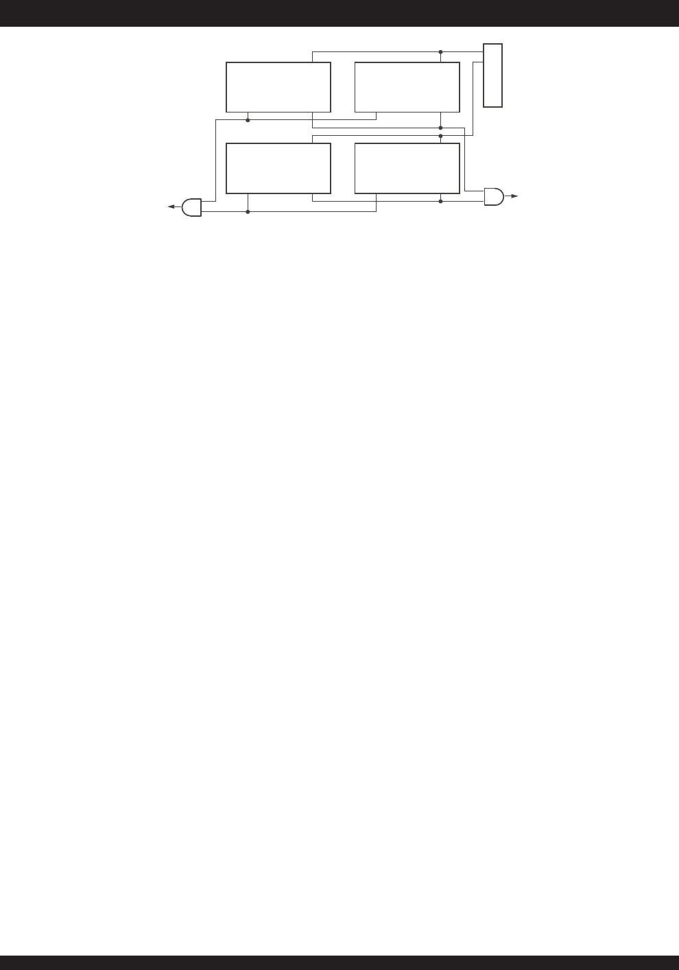
How the Semaphore Flags Work
The semaphore logic is a set of eight latches which are indepen-
dent of the Dual-Port SRAM. These latches can be used to pass a flag,
or token, from one port to the other to indicate that a shared resource
is in use. The semaphores provide a hardware assist for a use
assignment method called “Token Passing Allocation.” In this method,
the state of a semaphore latch is used as a token indicating that shared
resource is in use. If the left processor wants to use this resource, it
requests the token by setting the latch. This processor then verifies its
success in setting the latch by reading it. If it was successful, it
proceeds to assume control over the shared resource. If it was not
successful in setting the latch, it determines that the right side
processor has set the latch first, has the token and is using the shared
resource. The left processor can then either repeatedly request that
semaphore’s status or remove its request for that semaphore to
perform another task and occasionally attempt again to gain control of
the token via the set and test sequence. Once the right side has
relinquished the token, the left side should succeed in gaining control.
The semaphore flags are active low. A token is requested by writing
a zero into a semaphore latch and is released when the same side
writes a one to that latch.
The eight semaphore flags reside within the IDT70V05 in a
separate memory space from the Dual-Port SRAM. This address
space is accessed by placing a LOW input on the SEM pin (which acts
as a chip select for the semaphore flags) and using the other control
pins (Address, OE, and R/W) as they would be used in accessing a
standard Static RAM. Each of the flags has a unique address which can
be accessed by either side through address pins A
0 – A2. When accessing
the semaphores, none of the other address pins has any effect.
When writing to a semaphore, only data pin D
0 is used. If a LOW level
is written into an unused semaphore location, that flag will be set to a zero
on that side and a one on the other side (see Truth Table V). That
semaphore can now only be modified by the side showing the zero. When
a one is written into the same location from the same side, the flag will be
set to a one for both sides (unless a semaphore request from the other side
is pending) and then can be written to by both sides. The fact that the side
which is able to write a zero into a semaphore subsequently locks out writes
from the other side is what makes semaphore flags useful in interprocessor
communications. (A thorough discussion on the use of this feature follows
shortly.) A zero written into the same location from the other side will be
stored in the semaphore request latch for that side until the semaphore is
freed by the first side.
When a semaphore flag is read, its value is spread into all data bits so
that a flag that is a one reads as a one in all data bits and a flag containing
a zero reads as all zeros. The read value is latched into one side’s output
register when that side's semaphore select (SEM) and output enable (OE)
signals go active. This serves to disallow the semaphore from changing
state in the middle of a read cycle due to a write cycle from the other side.
Because of this latch, a repeated read of a semaphore in a test loop must
cause either signal (SEM or OE) to go inactive or the output will never
change.
A sequence WRITE/READ must be used by the semaphore in
order to guarantee that no system level contention will occur. A
processor requests access to shared resources by attempting to write
a zero into a semaphore location. If the semaphore is already in use,
the semaphore request latch will contain a zero, yet the semaphore
flag will appear as one, a fact which the processor will verify by the
subsequent read (see Truth Table V). As an example, assume a
processor writes a zero to the left port at a free semaphore location. On
a subsequent read, the processor will verify that it has written success-
fully to that location and will assume control over the resource in
question. Meanwhile, if a processor on the right side attempts to write
a zero to the same semaphore flag it will fail, as will be verified by the
fact that a one will be read from that semaphore on the right side during
subsequent read. Had a sequence of READ/WRITE been used
instead, system contention problems could have occurred during the
gap between the read and write cycles.
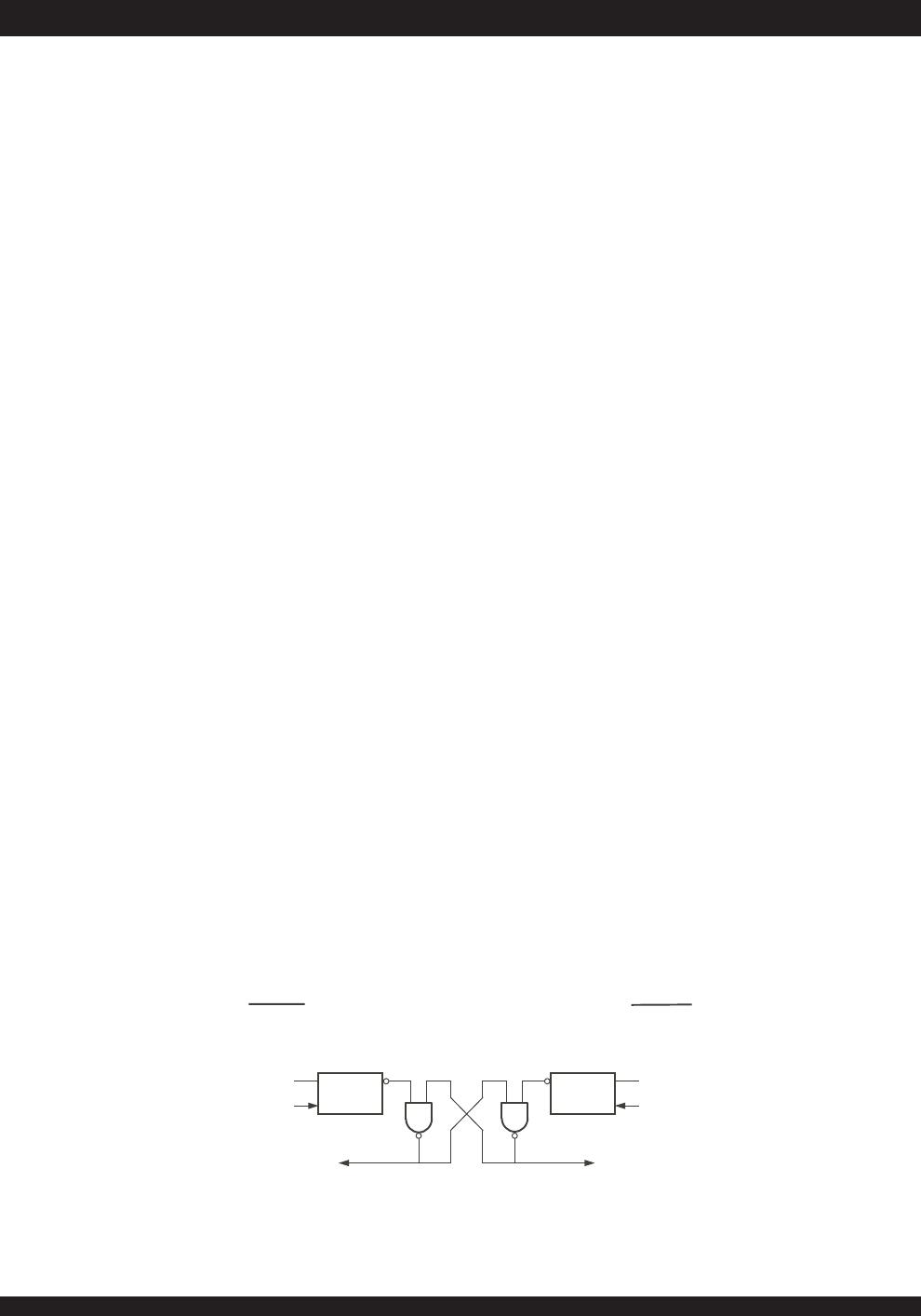
It is important to note that a failed semaphore request must be
followed by either repeated reads or by writing a one into the same
location. The reason for this is easily understood by looking at the
simple logic diagram of the semaphore flag in Figure 4. Two sema-
phore request latches feed into a semaphore flag. Whichever latch is
first to present a zero to the semaphore flag will force its side of the
semaphore flag LOW and the other side HIGH. This condition will
continue until a one is written to the same semaphore request latch.
Should the other side’s semaphore request latch have been written to
a zero in the meantime, the semaphore flag will flip over to the other
side as soon as a one is written into the first side’s request latch. The
second side’s flag will now stay LOW until its semaphore request latch
is written to a one. From this it is easy to understand that, if a
semaphore is requested and the processor which requested it no longer
needs the resource, the entire system can hang up until a one is written
into that semaphore request latch.
6.42
IDT70V05S/L
High-Speed 3.3V 8K x 8 Dual-Port Static RAM Industrial and Commercial Temperature Ranges
21
D
0
2941 drw 19
D
Q
WRITE
D
0
D
Q
WRITE
SEMAPHORE
REQUEST FLIP FLOP
SEMAPHORE
REQUEST FLIP FLOP
L PORT
R PORT
SEMAPHORE
READ
SEMAPHORE
READ
The critical case of semaphore timing is when both sides request a
single token by attempting to write a zero into it at the same time. The
semaphore logic is specially designed to resolve this problem. If
simultaneous requests are made, the logic guarantees that only one
side receives the token. If one side is earlier than the other in making
the request, the first side to make the request will receive the token. If
both requests arrive at the same time, the assignment will be arbitrarily
made to one port or the other.
One caution that should be noted when using semaphores is that
semaphores alone do not guarantee that access to a resource is
secure. As with any powerful programming technique, if semaphores
are misused or misinterpreted, a software error can easily happen.
Initialization of the semaphores is not automatic and must be
handled via the initialization program at power-up. Since any sema-
phore request flag which contains a zero must be reset to a one, all
semaphores on both sides should have a one written into them at
initialization from both sides to assure that they will be free when
needed.
Using Semaphores—Some Examples
Perhaps the simplest application of semaphores is their applica-
tion as resource markers for the IDT70V05’s Dual-Port SRAM. Say the
8K x 8 SRAM was to be divided into two 4K x 8 blocks which were to be
dedicated at any one time to servicing either the left or right port.
Semaphore 0 could be used to indicate the side which would control
the lower section of memory, and Semaphore 1 could be defined as the
indicator for the upper section of memory.
To take a resource, in this example the lower 4K of Dual-Port
SRAM, the processor on the left port could write and then read a
zero in to Semaphore 0. If this task were successfully completed
(a zero was read back rather than a one), the left processor would
assume control of the lower 4K. Meanwhile the right processor was
attempting to gain control of the resource after the left processor, it
would read back a one in response to the zero it had attempted to
write into Semaphore 0. At this point, the software could choose to try
and gain control of the second 4K section by writing, then reading a zero
into Semaphore 1. If it succeeded in gaining control, it would lock out
the left side.
Once the left side was finished with its task, it would write a one to
Semaphore 0 and may then try to gain access to Semaphore 1. If
Semaphore 1 was still occupied by the right side, the left side could undo
its semaphore request and perform other tasks until it was able to write, then
read a zero into Semaphore 1. If the right processor performs a similar task
with Semaphore 0, this protocol would allow the two processors to swap
4K blocks of Dual-Port SRAM with each other.
The blocks do not have to be any particular size and can even be
variable, depending upon the complexity of the software using the
semaphore flags. All eight semaphores could be used to divide the
Dual-Port SRAM or other shared resources into eight parts. Semaphores
can even be assigned different meanings on different sides rather than
being given a common meaning as was shown in the example above.
Semaphores are a useful form of arbitration in systems like disk
interfaces where the CPU must be locked out of a section of memory
during a transfer and the I/O device cannot tolerate any wait states.
With the use of semaphores, once the two devices has determined
which memory area was “off-limits” to the CPU, both the CPU and the
I/O devices could access their assigned portions of memory continu-
ously without any wait states.
Semaphores are also useful in applications where no memory
“WAIT” state is available on one or both sides. Once a semaphore
handshake has been performed, both processors can access their
assigned SRAM segments at full speed.
Another application is in the area of complex data structures. In this
case, block arbitration is very important. For this application one
processor may be responsible for building and updating a data
structure. The other processor then reads and interprets that data
structure. If the interpreting processor reads an incomplete data
structure, a major error condition may exist. Therefore, some sort of
arbitration must be used between the two different processors. The
building processor arbitrates for the block, locks it and then is able to
go in and update the data structure. When the update is completed, the
data structure block is released. This allows the interpreting processor
to come back and read the complete data structure, thereby guaran-
teeing a consistent data structure.
Figure 4. IDT70V05 Semaphore Logic

70V05L15PFG8

Mfr. #:
Manufacturer:
IDT
Description:
SRAM 8K x 8 3.3v Dual- Port Ram
Lifecycle:
New from this manufacturer.
Delivery:
DHL FedEx Ups TNT EMS
Payment:
T/T Paypal Visa MoneyGram Western Union