6.42
IDT70V05S/L
High-Speed 3.3V 8K x 8 Dual-Port Static RAM Industrial and Commercial Temperature Ranges
5
DC Electrical Characteristics Over the Operating
Temperature and Supply Voltage Range
(VDD = 3.3V ± 0.3V)
Recommended DC Operating
Conditions
Maximum Operating Temperature
and Supply Voltage
(1)
Absolute Maximum Ratings
(1)
Capacitance (TA = +25°C, f = 1.0MHz)
NOTES:
1. Stresses greater than those listed under ABSOLUTE MAXIMUM RATINGS may
cause permanent damage to the device. This is a stress rating only and functional
operation of the device at these or any other conditions above those indicated in
the operational sections of this specification is not implied. Exposure to absolute
maximum rating conditions for extended periods may affect reliability.
2. V
TERM must not exceed VDD + 0.3V.
NOTE:
1. This is the parameter T
A. This is the "instant on" case temperature.
NOTES:
1. V
IL> -1.5V for pulse width less than 10ns.
2. V
TERM must not exceed VDD +0.3V.
lobmySgnitaRlaicremmoC
lairtsudnI&
tinU
V
MRET
)2(
egatloVlanimreT
tcepseRhtiw
DNGot
6.4+ot5.0-V
T
SAIB
erutarepmeT
saiBrednU
521+ot55-
o
C
T
GTS
egarotS
erutarepmeT
051+ot56-
o
C
I
TUO
tuptuOCD
tnerruC
05Am
40lbt1492
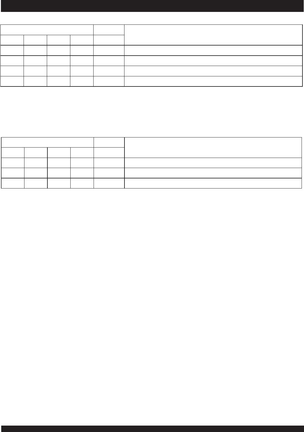
edarGerutarepmeTtneibmADNGVDD
laicremmoC0
O
07+otC
O
CV0V3.3
+
V3.0
lairtsudnI04-
O
58+otC
O
CV0V3.3
+
V3.0
50lbt1492
lobmySretemaraP.niM.pyT.xaMtinU
V
DD
egatloVylppuS0.33.36.3V
V
SS
dnuorG000V
V
HI
egatloVhgiHtupnI0.2
____
V
DD
3.0+
)2(
V
V
LI
egatloVwoLtupnI5.0-
)1(
____
8.0V
60lbt1492
lobmySretemaraP
)1(
snoitidnoC.xaMtinU
C
NI
ecnaticapaCtupnIV
NI
Vd3=9Fp
C
TUO
ecnaticapaCtuptuOV
TUO
Vd3=01Fp
70lbt1492
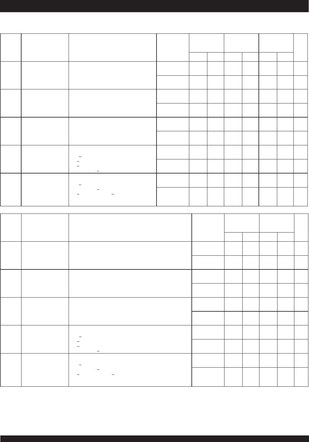
lobmySretemaraPsnoitidnoCtseT
S50V07L50V07
tinU.niM.xaM.niM.xaM
I|
LI
|tnerruCegakaeLtupnI
)1(
V
DD
V,V6.3=
NI
VotV0=
DD
___
01
___
5Aµ
I|
OL
|tnerruCegakaeLtuptuOV
TUO
VotV0=
DD
___
01
___
5Aµ
V
LO
egatloVwoLtuptuOI
LO
Am4+=
___
4.0
___
4.0V
V
HO
egatloVhgiHtuptuOI
HO
Am4-=4.2
___
4.2
___
V
80lbt1492
NOTES:
1. This parameter is determined by device characterization but is not production
tested.
2. 3dV references the interpolated capacitznce when the input and output signals
switch from 0V to 3V or from 3V to 0V.
NOTE:
1. At V
DD < 2.0V input leakages are undefined.