Data Sheet AD590
Rev. G | Page 7 of 16
EXPLANATION OF TEMPERATURE SENSOR
SPECIFICATIONS
The way in which the AD590 is specified makes it easy to apply
it in a wide variety of applications. It is important to understand
the meaning of the various specifications and the effects of the
supply voltage and thermal environment on accuracy.
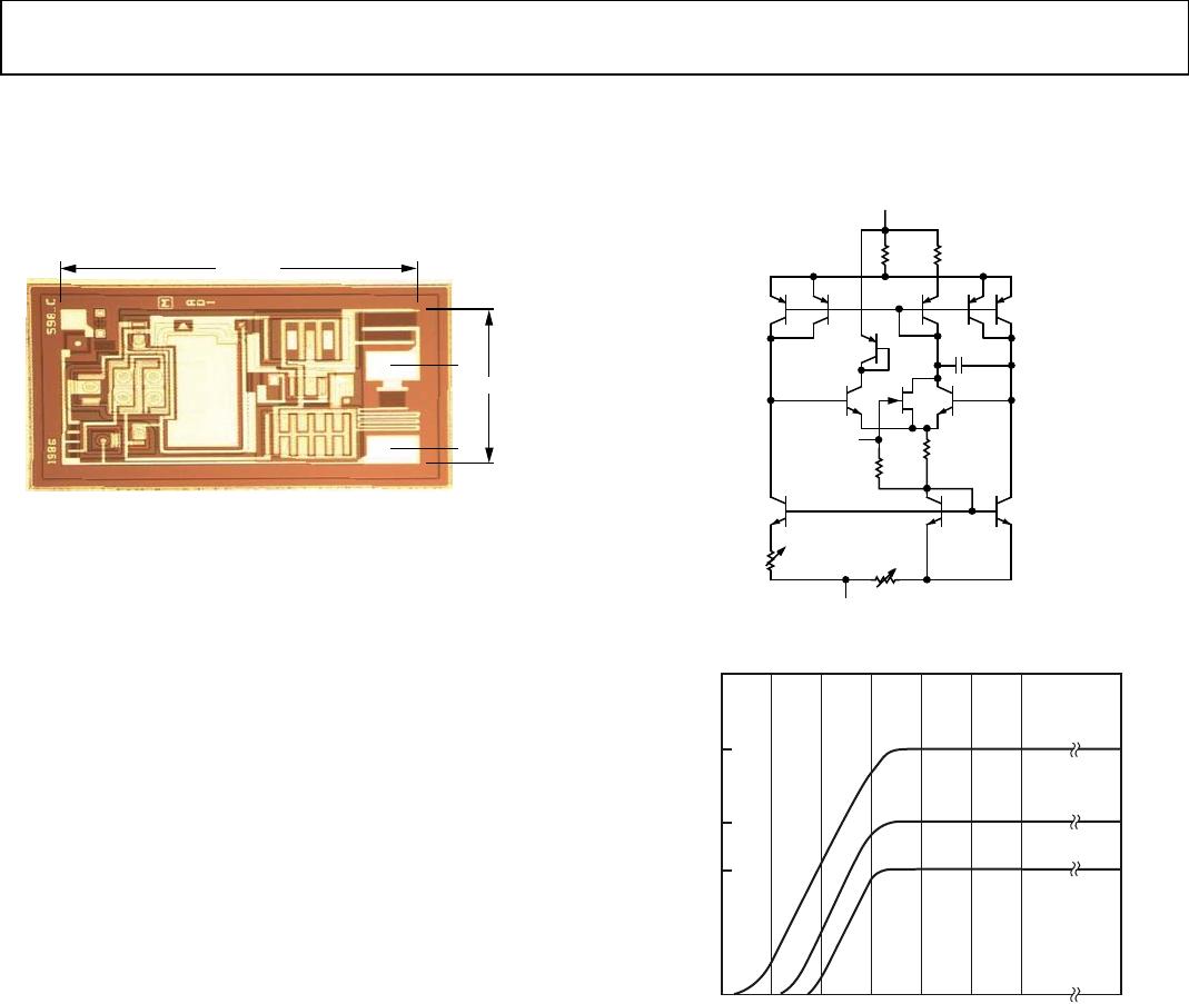
The AD590 is a PTAT current regulator. (Note that T (°C) =
T (K) − 273.2. Zero on the Kelvin scale is absolute zero; there is
no lower temperature.) That is, the output current is equal to a
scale factor times the temperature of the sensor in degrees
Kelvin. This scale factor is trimmed to 1 μA/K at the factory, by
adjusting the indicated temperature (that is, the output current)
to agree with the actual temperature. This is done with 5 V
across the device at a temperature within a few degrees of 25°C
(298.2 K). The device is then packaged and tested for accuracy
over temperature.
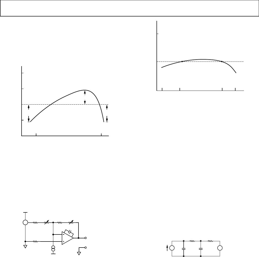
CALIBRATION ERROR
At final factory test, the difference between the indicated
temperature and the actual temperature is called the calibration
error. Since this is a scale factory error, its contribution to the
total error of the device is PTAT. For example, the effect of the
1°C specified maximum error of the AD590L varies from 0.73°C
at −55°C to 1.42°C at 150°C. Figure 9 shows how an exaggerated
calibration error would vary from the ideal over temperature.
Figure 9. Calibration Error vs. Temperature
The calibration error is a primary contributor to the maximum
total error in all AD590 grades. However, because it is a scale
factor error, it is particularly easy to trim. Figure 10 shows the
most elementary way of accomplishing this.
To trim this circuit, the temperature of the AD590 is measured
by a reference temperature sensor and R is trimmed so that V
T
= 1 mV/K at that temperature. Note that when this error is
trimmed out at one temperature, its effect is zero over the entire
temperature range. In most applications, there is a current-to-
voltage conversion resistor (or, as with a current input ADC, a
reference) that can be trimmed for scale factor adjustment.
Figure 10. One Temperature Trim
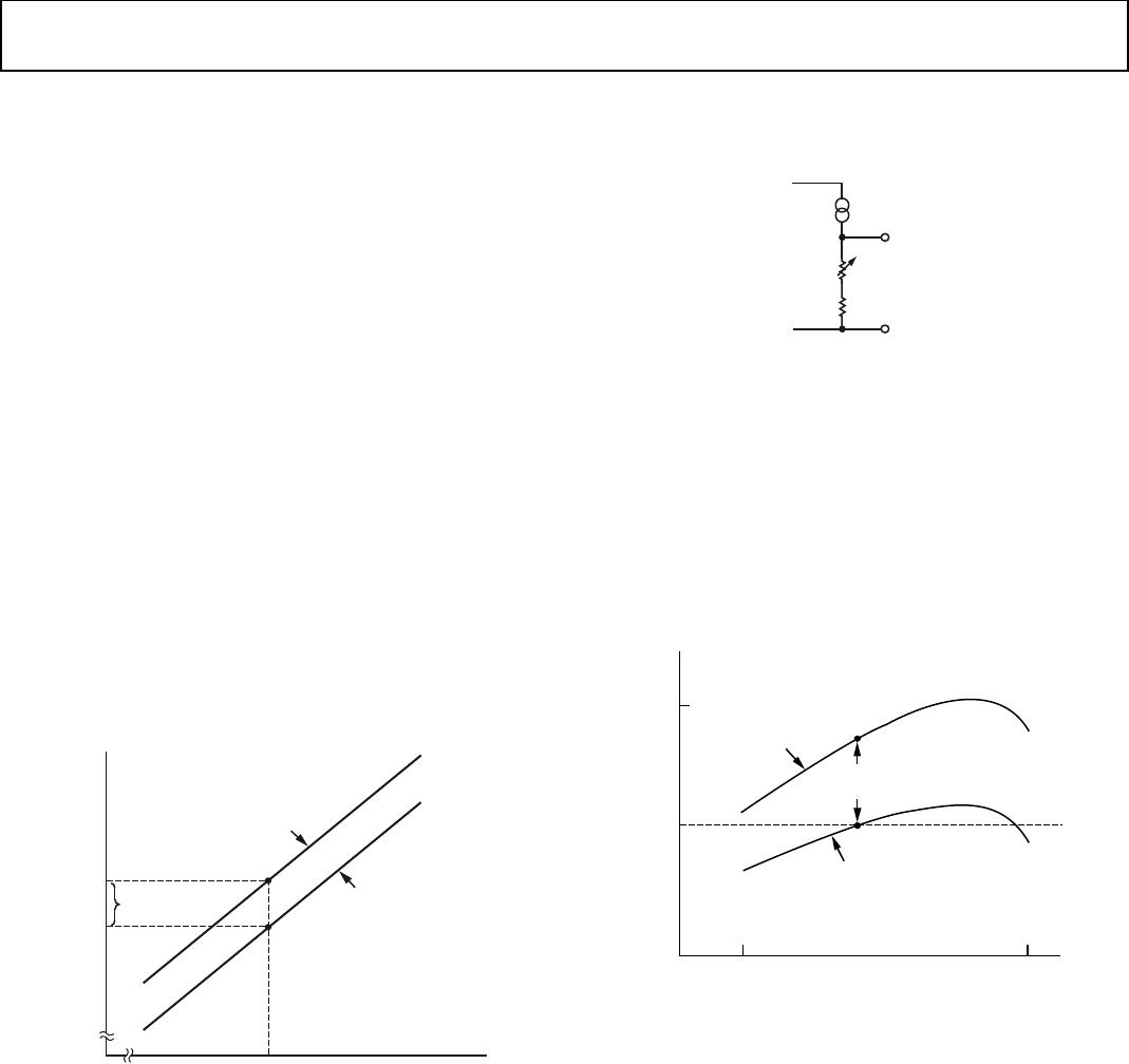
ERROR VS. TEMPERATURE: CALIBRATION ERROR
TRIMMED OUT
Each AD590 is tested for error over the temperature range with
the calibration error trimmed out. This specification could also
be called the variance from PTAT, because it is the maximum
difference between the actual current over temperature and a
PTAT multiplication of the actual current at 25°C. This error
consists of a slope error and some curvature, mostly at the
temperature extremes. Figure 11 shows a typical AD590K
temperature curve before and after calibration error trimming.
Figure 11. Effect to Scale Factor Trim on Accuracy
ERROR VS. TEMPERATURE: NO USER TRIMS
Using the AD590 by simply measuring the current, the total
error is the variance from PTAT, described above, plus the effect
of the calibration error over temperature. For example, the
AD590L maximum total error varies from 2.33°C at −55°C to
3.02°C at 150°C. For simplicity, only the large figure is shown
on the specification page.
00533-006
I
ACTUAL
298.2
I
OUT
µA)
298.2
TEMPERATURE (°K)
ACTUAL
TRANSFER
FUNCTION
IDEAL
TRANSFER
FUNCTION
CALIBRATION
ERROR
00533-007
5
R
100Ω
V
T
= 1mV/K
AD590
950Ω
+
–
+
–
+
–
AFTER
CALIBRATION
TRIM
00533-008
ABSOLUTE ERROR (°C)
2
0
–2
–55 150
TEMPERATURE (°C)
CALIBRATION
ERROR
BEFORE
CALIBRATION
TRIM