MAX3840ETJ+

MAX3840
+3.3V, 2.7Gbps Dual 2
2 Crosspoint Switch
4 _______________________________________________________________________________________
SUPPLY CURRENT vs. TEMPERATURE
MAX3840 toc01
0
20
60
40
120
140
100
80
160
SUPPLY CURRENT (mA)
-50 -10 10-30
30
50 70 90
TEMPERATURE (°C)
4 OUTPUTS ENABLED
3 OUTPUTS ENABLED
2 OUTPUTS ENABLED
1 OUTPUT ENABLED
0 OUTPUTS ENABLED
CML DIFFERENTIAL VOLTAGE
MAX3840 toc02
200
250
400
350
300
650
600
700
750
550
500
450
800
CML DIFFERENTIAL VOLTAGE (mV
P-P
)
-50 -10 10-30
30
50 70 90
TEMPERATURE (°C)
0
4
2
8
6
12
10
14
18
16
20
-50 -10-30 10 30 50 70 90
CHANNEL-TO-CHANNEL SKEW
vs. TEMPERATURE
MAX3840 toc04
TEMPERATURE (°C)
TMIE (ps)
CHANNEL A
CHANNEL B
2.7Gbps EYE DIAGRAM
MAX3840 toc03
54ps/div
150mV/div
INPUT = 2
23
- 1PRBS
Typical Operating Characteristics
(V
CC
= +3.3V, T
A
= +25°C, unless otherwise noted.)
MAX3840
+3.3V, 2.7Gbps Dual 2
2 Crosspoint Switch
_______________________________________________________________________________________ 5
Pin Description
PIN NAME FUNCTION
1 ENB1 Channel B1 Output Enable, TTL Input. A TTL low input powers down B1 output stage.
2 DIB1+ Channel B1 Positive Signal Input, CML
3 DIB1- Channel B1 Negative Signal Input, CML
4 ENB0 Channel B0 Output Enable, TTL Input. A TTL low input powers down B0 output stage.
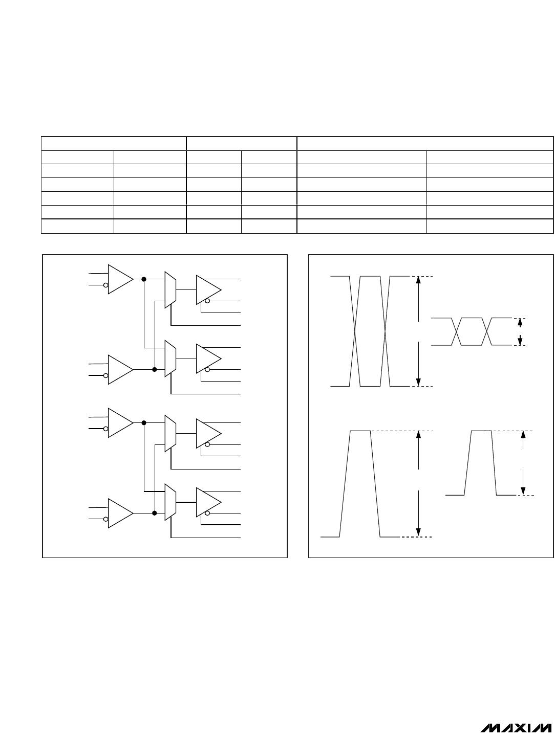
5 SELB0 Channel B0 Output Select, TTL Input. See Table 1.
6 DIB0+ Channel B0 Positive Signal Input, CML
7 DIB0- Channel B0 Negative Signal Input, CML
8 SELB1 Channel B1 Output Select, TTL Input. See Table 1.
9, 24 GND Supply Ground
10, 13, 16, 17,
20, 23
V
CC
Positive Supply
11 DOB0- Channel B0 Negative Output, CML
12 DOB0+ Channel B0 Positive Output, CML
14 DOB1- Channel B1 Negative Output, CML
15 DOB1+ Channel B1 Positive Output, CML
18 DOA1- Channel A1 Negative Output, CML
19 DOA1+ Channel A1 Positive Output, CML
21 DOA0- Channel A0 Negative Output, CML
22 DOA0+ Channel A0 Positive Output, CML
25 SELA1 Channel A1 Output Select, TTL Input. See Table 1.
26 DIA0+ Channel A0 Positive Signal Input, CML
27 DIA0- Channel A0 Negative Signal Input, CML
28 SELA0 Channel A0 Output Select, TTL Input. See Table 1.
29 ENA0 Channel A0 Output Enable, TTL Input. A TTL low input powers down A0 output stage.
30 DIA1+ Channel A1 Positive Signal Input, CML
31 DIA1- Channel A1 Negative Signal Input, CML
32 ENA1 Channel A1 Output Enable, TTL Input. A TTL low input powers down A1 output stage.
EP Exposed Pad
Ground. The exposed pad must be soldered to the circuit board ground for proper
electrical and thermal operation.
MAX3840
+3.3V, 2.7Gbps Dual 2
2 Crosspoint Switch
6 _______________________________________________________________________________________
_______________ Detailed Description
The block diagram in Figure 1 shows the MAX3840
architecture. The SELA_ and SELB_ pins control the rout-
ing of the signals through the crosspoint switch. Each
output of the crosspoint switch drives a CML output dri-
ver. Each of the outputs, DOA_ and DOB_, is enabled or
disabled by the respective ENA_ and ENB_ pins.
CML Inputs and Outputs
CML is used to simplify high-speed interfacing. On-
chip input and output terminations minimize the number
of external components required while improving signal
integrity. The CML output signal swing is small, result-
ing in lower power consumption. The internal 50Ω input
and output terminations minimize reflections and elimi-
nate the need for external terminations.
ROUTING CONTROLS OUTPUT CONTROLS OUTPUT SIGNALS
SELA0/SELB0
SELA1/SELB1 ENA0/ENA1 ENB0/ENB1
Signal at DOA0/DOB0 Signal at DOA1/DOB1
0 0 1 1 DIA0/DIB0 DIA0/DIB0
0 1 1 1 DIA0/DIB0 DIA1/DIB1
1 0 1 1 DIA1/DIB1 DIA0/DIB0
1 1 1 1 DIA1/DIB1 DIA1/DIB1
X X 0 0 Power Down Power Down
Table 1. Output Routing
DOA0+
0
1
0
1
DOA0-
ENA0
SELA0
CML
CML
DOA1+
DIA0-
DIA0+
DOA1-
ENA1
SELA1
CML
DIA1-
DIA1+
DOB0+
0
1
0
1
DOB0-
ENB0
SELB0
CML
DOB1+
DIB0-
DIB0+
DOB1-
ENB1
SELB1
CML
DIB1-
DIB1+
CML
CML
CML
320mV MIN
CML+
CML-
(CML+) - (CML-)
500mV
MAX
1000mV
MAX
640mV
MIN
Figure 1. Functional Block Diagram Figure 2. CML Output Levels

MAX3840ETJ+

Mfr. #:
Manufacturer:
Maxim Integrated
Description:
Analog & Digital Crosspoint ICs 3.3V 2.7Gbps Dual 2X2 Crx Switch
Lifecycle:
New from this manufacturer.
Delivery:
DHL FedEx Ups TNT EMS
Payment:
T/T Paypal Visa MoneyGram Western Union

Products related to this Datasheet