DATASHEET
9DMV0141 AUGUST 15, 2017 1 ©2017 Integrated Device Technology, Inc.
2:1 1.8V PCIe Gen1-2-3 Clock Mux with
Zo=100ohms
9DMV0141
Description
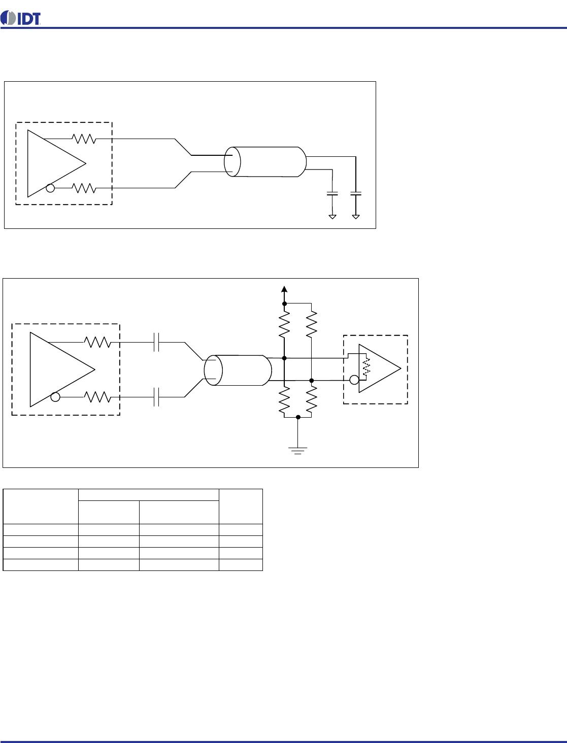
The 9DMV0141 is a member of IDT's SOC-Friendly 1.8V
Very-Low-Power (VLP) PCIe Gen1-2-3 family. It has
integrated output terminations providing Zo=100 for direct
connection to 100 transmission lines. The output has an
OE# pin for optimal system control and power management.
The part provides asynchronous or glitch-free switching
modes.
Typical Application
2:1 PCIe Gen1-2-3 Clock Multiplexer
Output Features
• 1 -Low-Power (LP) HCSL DIF pair w/ZO=100
Key Specifications
• DIF additive cycle-to-cycle jitter <5ps
• DIF phase jitter is PCIe Gen1-2-3 compliant
• 125MHz additive phase jitter 420fs rms typical (12kHz to
20MHz)
Features
• LP-HCSL output w/integrated terminations; saves 4
resistors compared to standard HCSL output
• 1.8V operation; 12mW typical power consumption
• Selectable asynchronous or glitch-free switching; allows
the mux to be selected at power up even if both inputs are
not running, then transition to glitch-free switching mode
• Spread Spectrum Compatible; supports EMI reduction
• OE# pins; support DIF power management
• HCSL differential inputs; can be driven by common clock
sources
• 1MHz to 200MHz operating frequency
• Configuration can be accomplished with strapping pins;
SMBus interface not required for device control
• Space saving 16-pin 3x3mm VFQFPN; minimal board
space
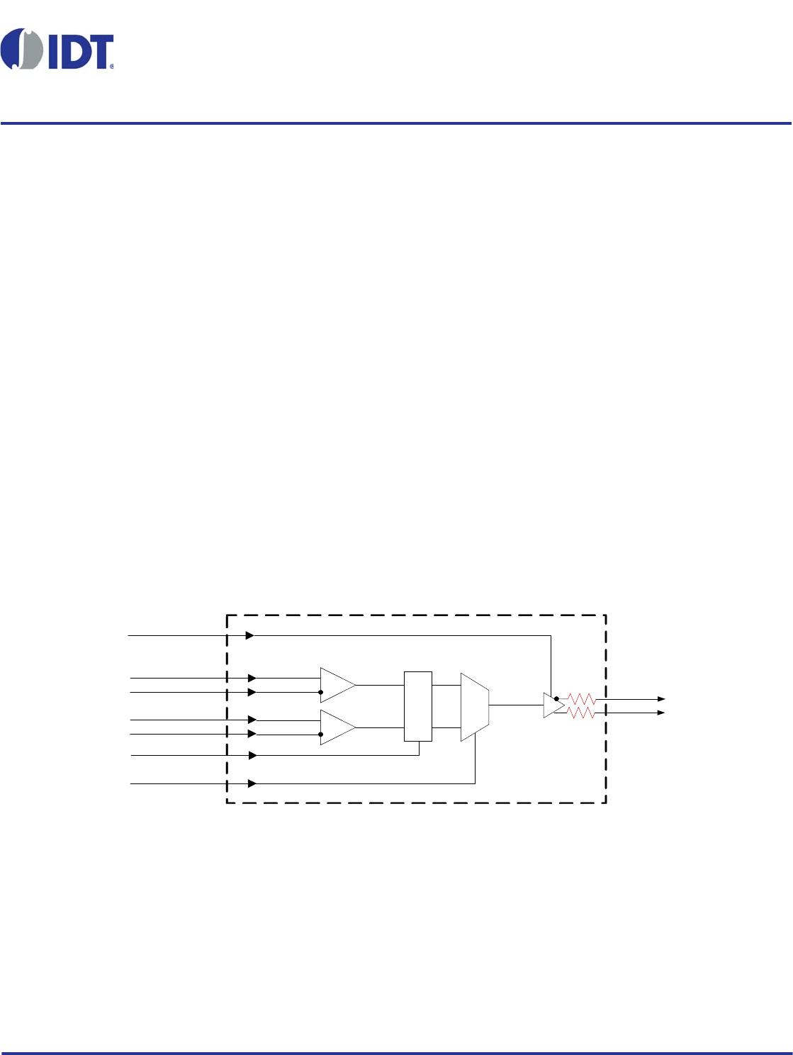
Block Diagram
A
B
DIF0
^OE0#
DIF_INA
DIF_INB
vSW_MODE
^SEL_A_B#