UPC8195K-A

UPC8195K
Applied Pin Functions and Applications Internal Equivalent Circuits
Pin Pin Voltage Voltage
No. Name (V) (V)
1QbV
CC/2 - Q signal input pin.
Apply bias voltage externally.
Maximum balance input voltage is
1 000 mV
p-p (balance).
2QV
CC/2 -
3 GND
(Shifter) 0 - Ground pin of I/Q modulator.
This pin should be grounded with
minimum inductance.
Form the ground pattern as widely as
possible to minimize ground impedance.
4 N.C. 0 - No connection
5
This pin is not connected to internal circuit
This pin should be opened or grounded.
6 LOb 0 2.02 Bypass pin of local signal input for I/Q
modulator.
In the case of single local input,
this pin must be decoupled with capacitor
ex. 1 000 pF.
7 LO 0 2.02 Local signal input of I/Q modulator.
The DC cut capacitor ex. 1 000 pF
must be attaced to this pin.
8V
CC 2.7 to 3.3 - Supply voltage pin of I/Q modulator.
(Shifter)
9VPS 0 to 3.0 - Power saving pin of I/Q modulator +
AGC amplifier.
This pin modulator can control
Active/Sleep state with bias as follows.
PIN FUNCTIONS (Pin Voltage is measured at VCC = 2.85 V)
VPS (V) State
0 to 0.5 Sleep Mode
2.2 to 3 Active Mode
1 2
9
50 k
UPC8195K
Applied Pin Functions and Applications Internal Equivalent Circuits
Pin Pin Voltage Voltage
No. Name (V) (V)
10 Vcont 0 to 3.0 - Gain control pin of AGC amplifier.
Variable gains are available in
accordance with applied voltage
between 0 to 3.0 V.
11 V
CC 2.7 to 3.3 - Supply voltage pin of internal regulator.
(REG.)
12 GND 0 - Ground pin internal regulator.
(REG.) This pin should be grounded with
minimum inductance.
Form the ground pattern as widely
as possible to minimize ground impedance.
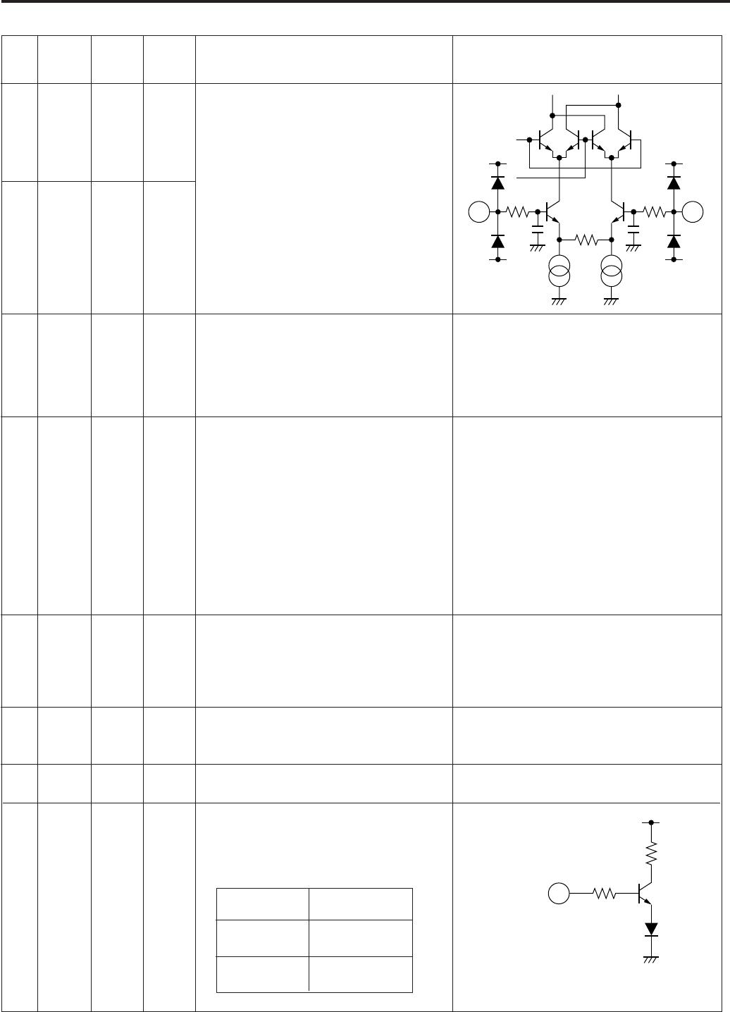
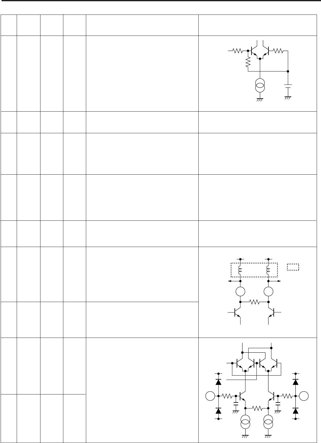
13 GND 0 - Ground pin of AGC amplifier + I/Q Mixer.
14 (AGC,
18 MIX) This pin should be grounded with
minimum inductance.
Form the ground pattern as widely
as possible to minimize ground impedance.
15 V
CC 2.7 to 3.3 - Supply voltage pin of AGC amplifier +
(AGC I/Q Mixer.
, MIX)
16 IFout 2.7 to 3.3 - IF output pin.
The inductor must be attached between
VCC and output pin due to open collector.
Output frequency is 570 MHz which is
3/4 of local signal frequency 760 MHz.
17 IFoutb 2.7 to 3.3 - Balance output of IFout pin.
The inductor must be attached between
VCC and output pin due to open collector.
19 I VCC/2 - I signal input pin.
Apply bias voltage externally.
Maximum balance input voltage is
1 000 mVP-P (balance).
20 Ib VCC/2 -
PIN FUNCTIONS (Pin Voltage is measured at VCC = 2.85 V)
10.5 k
2.5 k
1716
External
1 k
19 20
UPC8195K
EXCLUSIVE NORTH AMERICAN AGENT FOR NEC RF, MICROWAVE & OPTOELECTRONIC SEMICONDUCTORS
CALIFORNIA EASTERN LABORATORIES • Headquarters • 4590 Patrick Henry Drive • Santa Clara, CA 95054-1817 • (408) 988-3500 • Telex 34-6393 • FAX (408) 988-0279
Internet: http://WWW.CEL.COM
04/15/2002
DATA SUBJECT TO CHANGE WITHOUT NOTICE
0.8±0.1
4.2±0.2
4.2±0.2
3.0±0.2
4.2±0.2
4.0±0.2
3.2±0.2
Pin 20
Pin 1
4-C0.5
3.2±0.2
3.0±0.2
0.30±0.15
0.18±0.05
0.4
Package Outline QFN-20
OUTLINE DIMENSIONS (Units in mm)
APPLICATION EXAMPLE: W-CDMA
Variation of IF plan
UPC8190/91K: RX-IF = 380 MHz, TX-IF = 570 MHz
UPC8194/95K: RX-IF = 190 MHz, TX-IF = 380 MHz
BPF
PA
AGC + PA Driver
UPG2124TH
MIX
1st LO
2nd LO = 760 MHz
DUPLX
ANTENNA
AGC+IQ demodulator
UPC8190K, 8194K
AGC+IQ modulator
UPC8191K, 8195K
BPF
BPF
BPF
LNA
MIX
PLL1
PLL2
SiMMIC
GaAs MMIC
GaAs or Si Discrete
GaAs MCM
TX = 1920-1980 MHz
RX = 2110-2170 MHz
To
Baseband
From
Baseband
Life Support Applications
These NEC products are not intended for use in life support devices, appliances, or systems where the malfunction of these products can reasonably
be expected to result in personal injury. The customers of CEL using or selling these products for use in such applications do so at their own risk and
agree to fully indemnify CEL for all damages resulting from such improper use or sale.

UPC8195K-A

Mfr. #:
Manufacturer:
CEL
Description:
RF Transmitter TX-IF AGC + I/Q Mod
Lifecycle:
New from this manufacturer.
Delivery:
DHL FedEx Ups TNT EMS
Payment:
T/T Paypal Visa MoneyGram Western Union

Products related to this Datasheet