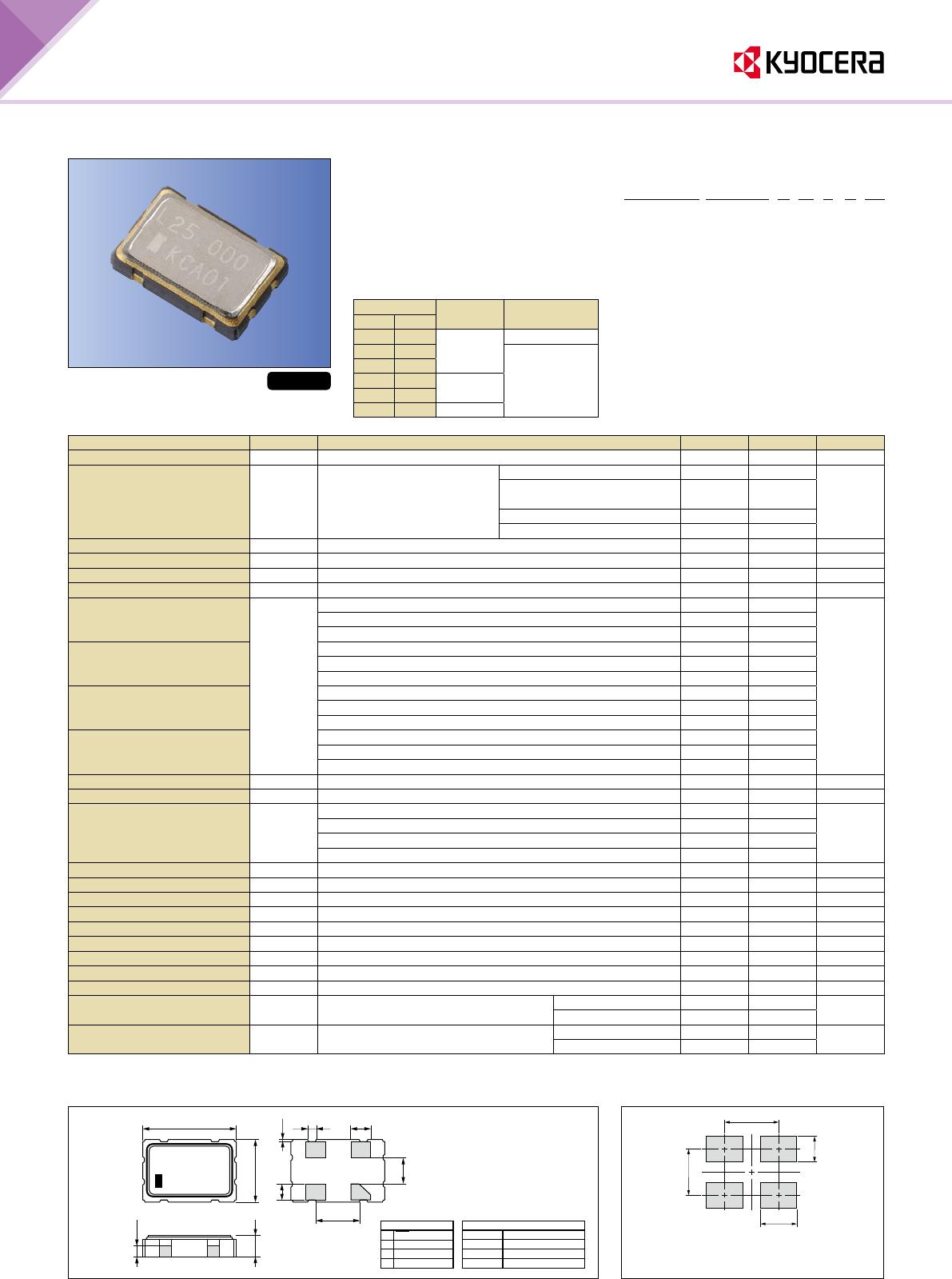
Clock Oscillators Surface Mount Type
KC5032A-CM Series
CMOS/ 1.8V
〜
5.0V/ 5.0
×
3.2mm
Features
•
Wide operating voltage range 1.6 to 5.5V
•
±
25
×
10
−
6
available
• Highly reliable with seam welding
• Miniature ceramic package
• CMOS output
Table 1
Freq. Tol.
Operating
Temperature
Range (
°
C)
Note
Code
×
10
−
6
0
±
50
−
10 to
+
70
Standard specications
S
±
30
With only certain
frequencies
U
±
25
F
±
100
−
40 to
+
85
G
±
50
6
±
50
−
40 to
+
105
How to Order
KC5032A 25.0000 C M 0 E 00
① ② ③ ④ ⑤ ⑥ ⑦
①
Series
②
Output Frequency
③
Output Type (CMOS)
④
Supply Voltage (1.8V, 2.5V, 3.3V, 5V Compatible)
⑤
Frequency Tolerance (See Table 1)
⑥
Symmetry/ INH Function
(45/ 55%, Stand-by)
⑦
Customer Special Model Sufx
(STD Specication is “00”)
Packaging (Tape & Reel 1000 pcs./ reel)
Specifications
Item Symbol Conditions Min. Max. Units
Output Frequency Range fo 1.8 50 MHz
Frequency Tolerance f
_tol
Initial tolerance, Operating
temperature range, Rated
power supply voltage change,
Load change, Aging (1 year
@25
°
C), Shock and vibration
Op. Temp.:
−
40 to
+
85
°
C
−
100
+
100
×
10
−
6
Op. Temp.:
−
10 to
+
70
°
C/
−
40 to
+
85
°
C/
−
40 to
+
105
°
C
−
50
+
50
Op. Temp.:
−
10 to
+
70
°
C
−
30
+
30
Op. Temp.:
−
10 to
+
70
°
C
−
25
+
25
Storage Temperature Range T
_stg
−
55
+
125
°
C
Operating Temperature Range
T_use
−
40
+
105
°
C
Max. Supply Voltage —
−
0.6
+
6.5 V
Supply Voltage V
CC
+
1.6
+
5.5 V
Current Consumption (Loaded)
(1.6
≤
VCC
≤
2.0V)
I
CC
1.8
≤
fo
≤
20MHz — 3.5
mA
20
<
fo
≤
40MHz — 4.5
40
<
fo
≤
50MHz — 5.0
Current Consumption (Loaded)
(2.0
<
VCC
≤
2.8V)
1.8
≤
fo
≤
20MHz — 4.0
20
<
fo
≤
40MHz — 5.0
40
<
fo
≤
50MHz — 6.0
Current Consumption (Loaded)
(2.8
<
VCC
≤
3.63V)
1.8
≤
fo
≤
20MHz — 5.0
20
<
fo
≤
40MHz — 6.0
40
<
fo
≤
50MHz — 7.0
Current Consumption (Loaded)
(3.63
<
VCC
≤
5.5V)
1.8
≤
fo
≤
20MHz — 7.0
20
<
fo
≤
40MHz — 8.0
40
<
fo
≤
50MHz — 9.5
Stand-by Current I
_std — 10
μ
A
Symmetry SYM @50% V
CC 45 55 %
Rise/ Fall Time
(10% VCC to 90% VCC Maximum Loaded)
tr/ tf
1.6
≤
V
CC
≤
2V — 8
ns
2<V
CC
≤
2.8V — 7
2.8<V
CC
≤
3.63V — 6
4.5
≤
V
CC
≤
5.5V — 5
Low Level Output Voltage V
OL IOL
=
4mA — 10% V
CC V
High Level Output Voltage V
OH IOH
=−
4mA 90% V
CC — V
Output Load L_CMOS 1.6
≤
V
CC
≤
5.5V — 15 pF
Input Voltage Range V
IN 0 VCC V
Low Level Input Voltage V
IL — 30% VCC V
High Level Input Voltage V
IH 70% VCC — V
Disable Time t
_dis — 150 ns
Enable Time t
_ena — 5 ms
Start-up Time t
_str @Minimum operating voltage to be 0 sec. — 10 ms
1 Sigma Jitter J
Sigma Measured with Wavecrest SIA-3000
1.8
≤
fo
≤
40MHz — 8
ps
40
<
fo
≤
50MHz — 5
Peak to Peak Jitter J
PK-PK Measured with Wavecrest SIA-3000
1.8
≤
fo
≤
40MHz — 80
ps
40
<
fo
≤
50MHz — 50
Note: All electrical characteristics are defined at the maximum load and operating temperature range.
Please contact us for inquiry about operating temperature range, available frequencies and other conditions.
Dimensions (Unit: mm)
Recommended Land Pattern
(Unit: mm)
Plating: Ni+Au
Tolerance: ±0.2
Pad Connections
#1
INH
#2 Case GND
#3 Output
#4 V
CC
INH Function
Pad1 Pad3 (Output)
Open Active
"H" Level Active
"L" Level
High Z (No-Oscillation)
5.0
3.2
1.2
0.1
0 .5 1.2
0.5
1.0
2.5
#1#2
#3 #4
0.9
Note: A capacitor of value 0.01µF between VCC
and GND is recommended.
2.5
1.4
2.2
1.6
RoHS Compliant