MAX7409/MAX7410/MAX7413/MAX7414
5th-Order, Lowpass,
Switched-Capacitor Filters
4 _______________________________________________________________________________________
C
OSC
= 1000pF (Note 3)
CONDITIONS
21 30 38f
OSC
Internal Oscillator Frequency
MIN TYP MAX
SYMBOLPARAMETER
IN = COM (Note 4)
SHDN = GND
Operating mode, no load
V
CLK
= 0 or 3V
0.5V
SDL
SHDN Input Low
2.5V
SDH
SHDN Input High
70PSRRPower-Supply Rejection Ratio
0.2 1I
SHDN
Shutdown Current
1.2 1.5
2.7 3.6V
DD
Supply Voltage
0.5V
IL
Clock Input Low
2.5V
IH
Clock Input High
±13.5 ±20I
CLK
Clock Output Current
(Internal Oscillator Mode)
V
V
dB
µA
V
V
V
µA
kHz
UNITS
SHDN Input Leakage Current
V
SHDN
= 0 to V
DD
0.2 ±10 µA
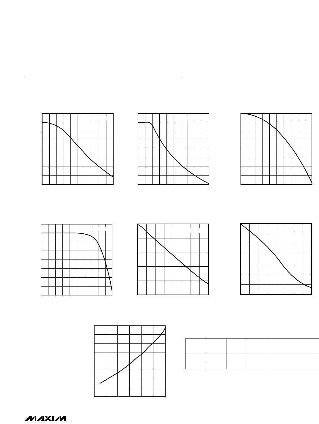
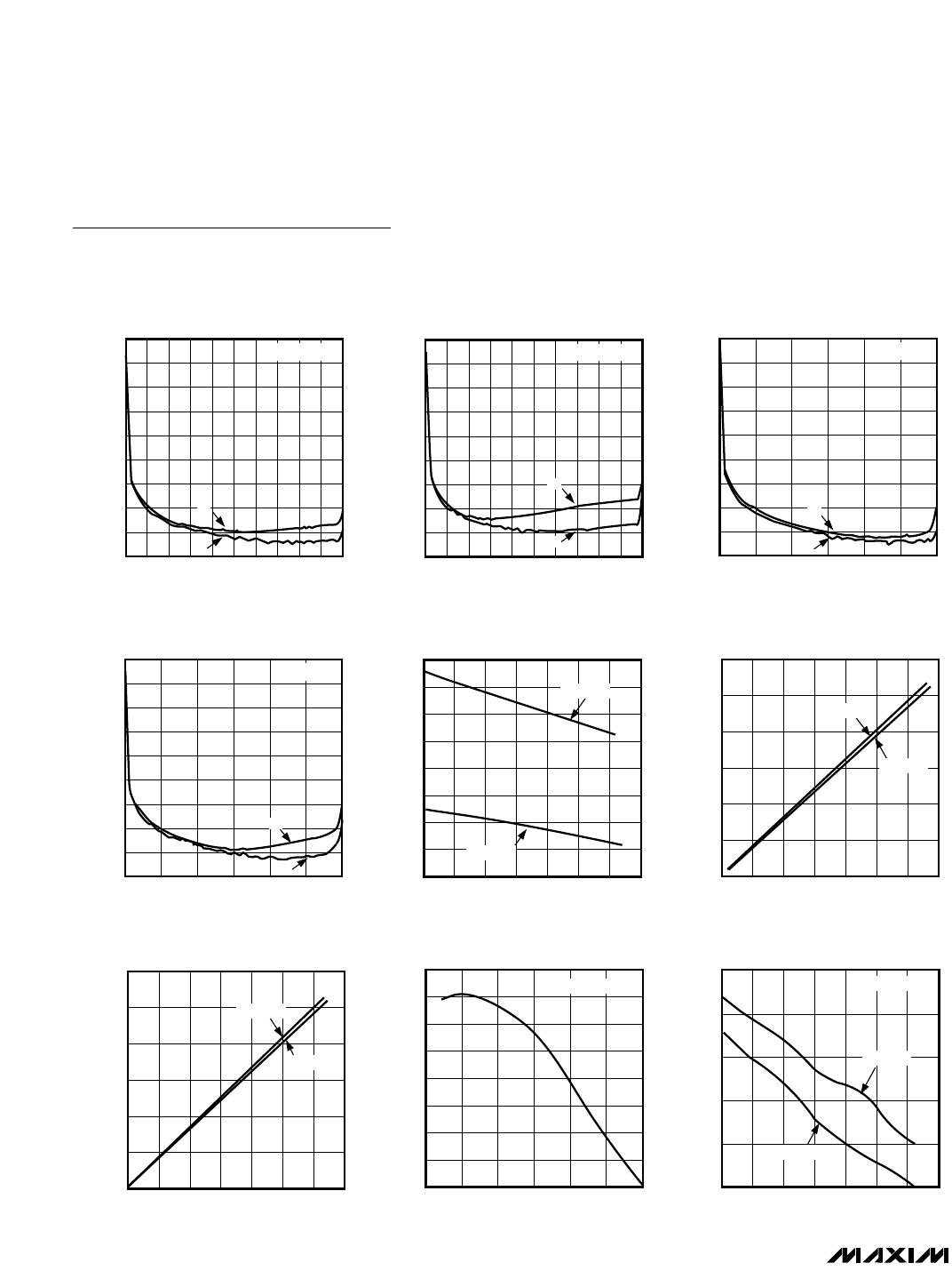
FILTER CHARACTERISTICS
(V
DD
= +5V for MAX7409/MAX7410, V
DD
= +3V for MAX7413/MAX7414, filter output measured at OUT, 10kΩ || 50pF load to GND at
OUT, SHDN = V
DD
, f
CLK
= 100kHz, T
A
= T
MIN
to T
MAX
, unless otherwise noted.)
Note 1: The maximum f
C
is defined as the clock frequency f
CLK
= 100 x f
C
at which the peak S / (THD+N) drops to 68dB with a
sinusoidal input at 0.2f
C
.
Note 2: DC insertion gain is defined as ∆V
OUT
/ ∆V
IN
.
Note 3: f
OSC
(kHz) ≅ 30 x 10
3
/ C
OSC
(pF).
Note 4: PSRR is the change in output voltage from a V
DD
of 4.5V and a V
DD
of 5.5V.
CLOCK
POWER REQUIREMENTS
SHUTDOWN
CONDITIONS UNITS
MIN TYP MAX
PARAMETER
mAI
DD
Supply Current
ELECTRICAL CHARACTERISTICS—MAX7413/MAX7414 (continued)
(V
DD
= +3V, filter output measured at OUT pin, 10kΩ || 50pF load to GND at OUT, OS = COM, 0.1µF capacitor from COM to GND,
SHDN = V
DD
, f
CLK
= 100kHz, T
A
= T
MIN
to T
MAX
, unless otherwise noted. Typical values are at T
A
= +25°C.)
f
IN
= 0.5f
C
-1 -0.74
f
IN
= f
C
-3.6 -3.0 -2.4
f
IN
= 4f
C
-41.0 -35
f
IN
= 7f
C
dB
-64.3 -58
f
IN
= 0.5f
C
dB
-0.3 0
f
IN
= 3f
C
f
IN
= f
C
-3.6 -3.0 -2.4
Insertion Gain Relative to
DC Gain
-47.5 -43
f
IN
= 5f
C
-70 -65
Insertion Gain Relative to
DC Gain
BESSEL FILTERS—MAX7409/MAX7413
BUTTERWORTH FILTERS—MAX7410/MAX7414