MAX7409/MAX7410/MAX7413/MAX7414
5th-Order, Lowpass,
Switched-Capacitor Filters
_______________________________________________________________________________________ 7
NAME FUNCTION
1 COM
Common Input Pin. Biased internally at midsupply. Bypass COM externally to GND with a 0.1µF capacitor.
To override internal biasing, drive COM with an external supply.
2 IN Filter Input
PIN
3 GND Ground
4 V
DD
Positive Supply Input: +5V for MAX7409/MAX7410, +3V for MAX7413/MAX7414.
8 CLK
Clock Input. Connect an external capacitor (C
OSC
) from CLK to ground: f
OSC
(kHz) = 30 x 10
3
/ C
OSC
(pF).
To override the internal oscillator, connect CLK to an external clock: f
C
= f
CLK
/100.
7
SHDN
Shutdown Input. Drive low to enable shutdown mode; drive high or connect to V
DD
for normal operation.
6 OS
Offset Adjust Input. To adjust output offset, connect OS to an external supply through a resistive voltage-
divider (Figure 3). Connect OS to COM if no offset adjustment is needed. Refer to the
Offset and Common-
Mode Input Adjustment
section.
5 OUT Filter Output
Pin Description
_______________Detailed Description
The MAX7409/MAX7413 Bessel filters provide low over-
shoot and fast settling responses, and the MAX7410/
MAX7414 Butterworth filters provide a maximally flat
passband response. All parts operate with a 100:1
clock-to-corner frequency ratio and a 15kHz maximum
corner frequency.
Bessel Characteristics
Lowpass Bessel filters such as the MAX7409/MAX7413
delay all frequency components equally, preserving the
shape of step inputs (subject to the attenuation of the
higher frequencies). Bessel filters settle quickly—an
important characteristic in applications that use a multi-
plexer (mux) to select an input signal for an analog-to-
digital converter (ADC). An anti-aliasing filter placed
between the mux and the ADC must settle quickly after
a new channel is selected.
Butterworth Characteristics
Lowpass Butterworth filters such as the MAX7410/
MAX7414 provide a maximally flat passband response,
making them ideal for instrumentation applications that
require minimum deviation from the DC gain throughout
the passband.
Typical Operating Characteristics (continued)
(V
DD
= +5V for MAX7409/MAX7410, V
DD
= +3V for MAX7413/MAX7414, f
CLK
= 100kHz, SHDN = V
DD
, COM = OS = V
DD
/ 2, T
A
= +25°C,
unless otherwise noted.)
-4.50
-4.00
-4.25
-3.50
-3.75
-3.25
-3.00
-40 20 40-20 0 60 80 100
OUTPUT OFFSET VOLTAGE
vs. TEMPERATURE
MAX7409 toc17
TEMPERATURE (°C)
OFFSET VOLTAGE (mV)
V
DD
= +3V
V
DD
= +5V
-5.0
-4.0
-4.5
-3.0
-3.5
-2.5
-2.0
2.5 3.5 4.03.0 4.5 5.0 5.5
OUTPUT OFFSET VOLTAGE
vs. SUPPLY VOLTAGE
MAX7409 toc18
SUPPLY VOLTAGE (V)
DC OFFSET VOLTAGE (mV)
MAX7409/MAX7410/MAX7413/MAX7414
5th-Order, Lowpass,
Switched-Capacitor Filters
8 _______________________________________________________________________________________
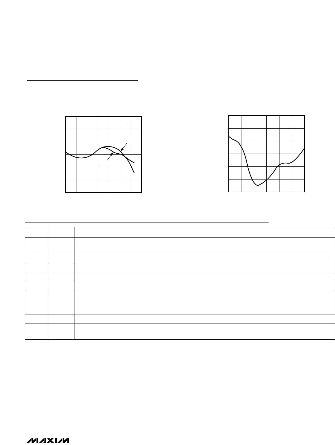
The difference between Bessel and Butterworth filters
can be observed when a 1kHz square wave is applied
to the filter input (Figure 1, trace A). With the filter cutoff
frequencies set at 5kHz, trace B shows the Bessel filter
response and trace C shows the Butterworth filter
response.
Background Information
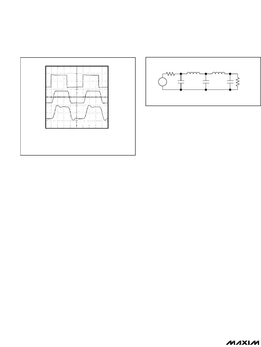
Most switched-capacitor filters (SCFs) are designed with
biquadratic sections. Each section implements two filter-
ing poles, and the sections are cascaded to produce
higher-order filters. The advantage to this approach is
ease of design. However, this type of design is highly
sensitive to component variations if any section’s Q is
high. An alternative approach is to emulate a passive net-
work using switched-capacitor integrators with summing
and scaling. Figure 2 shows a basic 5th-order ladder filter
structure.
A switched-capacitor filter such as the MAX7409/
MAX7410/MAX7413/MAX7414 emulates a passive ladder
filter. The filter’s component sensitivity is low when com-
pared to a cascaded biquad design, because each
component affects the entire filter shape, not just one
pole-zero pair. In other words, a mismatched component
in a biquad design will have a concentrated error on its
respective poles, while the same mismatch in a ladder
filter design results in an error distributed over all poles.
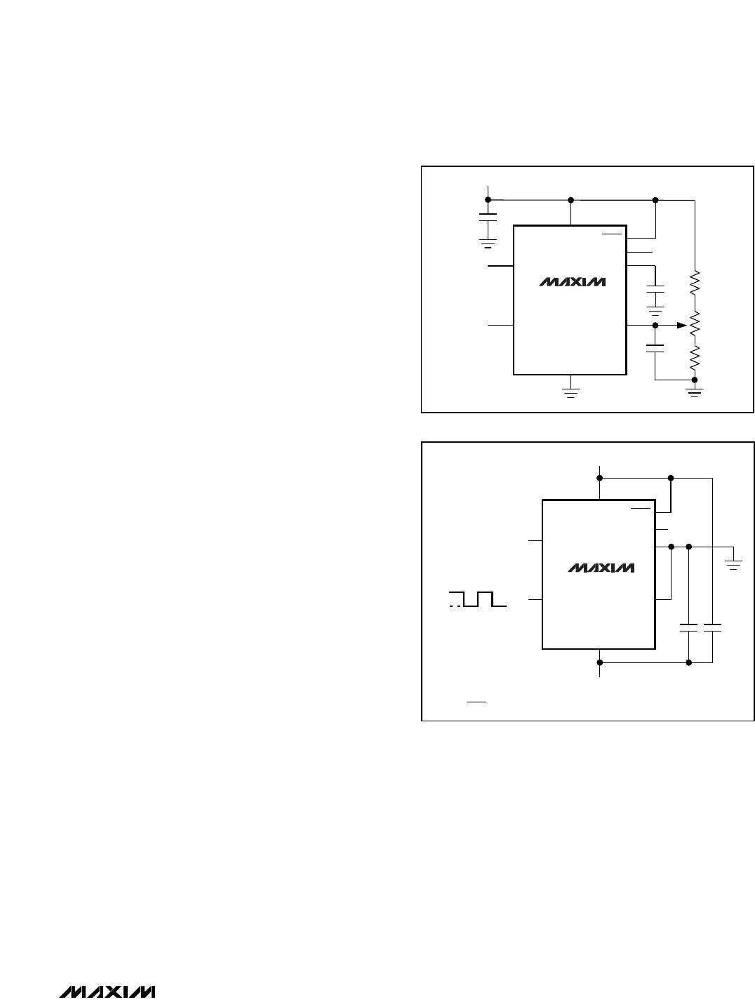
Clock Signal
External Clock
The MAX7409/MAX7410/MAX7413/MAX7414 family of
SCFs is designed for use with external clocks that have
a 50% ±10% duty cycle. When using an external clock
with these devices, drive CLK with a CMOS gate pow-
ered from 0 to V
DD
. Varying the rate of the external
clock adjusts the corner frequency of the filter as fol-
lows:
f
C
= f
CLK
/ 100
Internal Clock
When using the internal oscillator, connect a capacitor
(C
OSC
) between CLK and ground. The value of the
capacitor determines the oscillator frequency as follows:
f
OSC
(kHz) = 30 x 10
3
/ C
OSC
(pF)
Minimize the stray capacitance at CLK so that it does
not affect the internal oscillator frequency. Vary the rate
of the internal oscillator to adjust the filter’s corner fre-
quency by a 100:1 clock-to-corner frequency ratio. For
example, an internal oscillator frequency of 100kHz
produces a nominal corner frequency of 1kHz.
Input Impedance vs. Clock Frequencies
The MAX7409/MAX7410/MAX7413/MAX7414’s input
impedance is effectively that of a switched-capacitor
resistor (see the following equation), and is inversely
proportional to frequency. The input impedance values
determined below represent the average input imped-
ance, since the input current is not continuous. As a
rule, use a driver with an output impedance less than
10% of the filter’s input impedance. Estimate the input
impedance of the filter using the following formula:
Z
IN
= 1 / ( f
CLK
x 2.1pF)
For example, an f
CLK
of 100kHz results in an input
impedance of 4.8M.
L4
C5C3
C1
V
IN
+
-
R
L
L2
R
S
Figure 2. 5th-Order Ladder Filter Network
A
2V/div
2V/div
2V/div
C
A: 1kHz INPUT SIGNAL
B: MAX7409 BESSEL FILTER RESPONSE; f
C
= 5kHz
C: MAX7410 BUTTERWORTH FILTER RESPONSE; f
C
= 5kHz
B
200µs/div
Figure 1. Bessel vs. Butterworth Filter Response
MAX7409/MAX7410/MAX7413/MAX7414
5th-Order, Lowpass,
Switched-Capacitor Filters
_______________________________________________________________________________________ 9
Low-Power Shutdown Mode
These devices feature a shutdown mode that is activat-
ed by driving SHDN low. In shutdown mode, the filter’s
supply current reduces to 0.2µA and its output becomes
high impedance. For normal operation, drive SHDN
high or connect it to V
DD
.
__________Applications Information
Offset and Common-Mode
Input Adjustment
The COM pin sets the common-mode input voltage and
is biased at mid-supply with an internal resistor-divider.
If the application does not require offset adjustment,
connect OS to COM. For applications requiring offset
adjustment, apply an external bias voltage through a
resistor-divider network to OS such as shown in Fig-
ure 3. For applications that require DC level shifting,
adjust OS with respect to COM. (Note: OS should not
be left unconnected.) The output voltage is represent-
ed by this equation:
V
OUT
= (V
IN
- V
COM
) + V
OS
with V
COM
= V
DD
/ 2 (typical), and where (V
IN
- V
COM
)
is lowpass filtered by the SCF, and OS is added at the
output stage. See the
Electrical Characteristics
for the
voltage range of COM and OS. Changing the voltage
on COM or OS significantly from midsupply reduces
the filter’s dynamic range.
Power Supplies
The MAX7409/MAX7410 operate from a single +5V
supply and the MAX7413/MAX7414 operate from a sin-
gle +3V supply. Bypass V
DD
to GND with a 0.1µF
capacitor. If dual supplies are required (±2.5V for
MAX7409/MAX7410, ±1.5V for MAX7413/MAX7414),
connect COM to system ground and connect GND to
the negative supply. Figure 4 shows an example of
dual-supply operation. Single- and dual-supply perfor-
mance are equivalent. For either single- or dual-supply
operation, drive CLK and SHDN from GND (V- in dual-
supply operation) to V
DD
. For ±5V dual-supply applica-
tions, use the MAX291–MAX297.
Input Signal Amplitude Range
The optimal input signal range is determined by
observing the voltage level at which the Total Harmonic
Distortion + Noise is minimized for a given corner fre-
quency. The
Typical Operating Characteristics
show
graphs of the devices’ Total Harmonic Distortion plus
Noise Response as the input signal’s peak-to-peak
amplitude is varied.
Anti-Aliasing and DAC Postfiltering
When using these devices for anti-aliasing or DAC
postfiltering, synchronize the DAC (or ADC) and the fil-
ter clocks. If the clocks are not synchronized, beat fre-
quencies will alias into the desired passband.
Harmonic Distortion
Harmonic distortion arises from nonlinearities within the
filter. These nonlinearities generate harmonics when a
pure sine wave is applied to the filter input. Table 1 lists
typical harmonic-distortion values for the MAX7410/
MAX7414 with a 10kload at T
A
= +25°C. Table 2 lists
typical harmonic-distortion values for the MAX7409/
MAX7413 with a 10kload at T
A
= +25°C.
V
DD
V
SUPPLY
IN
CLK
GND
INPUT
OUTPUT
50k
50k
50k
OUT
0.1µF
0.1µF
0.1µF
CLOCK
SHDN
COM
OS
MAX7409
MAX7410
MAX7413
MAX7414
Figure 3. Offset Adjustment Circuit
V
DD
V+
V-
IN
CLK
GND
INPUT
OUTPUTOUT
0.1µF
CLOCK
*DRIVE SHDN TO V- FOR LOW-POWER SHUTDOWN MODE.
SHDN
COM
OS
0.1µF
MAX7409
MAX7410
MAX7413
MAX7414
*
V+
V-
Figure 4. Dual-Supply Operation

MAX7414CUA+

Mfr. #:
Manufacturer:
Maxim Integrated
Description:
Active Filter 5th-Order Lowpass Elliptic Filter
Lifecycle:
New from this manufacturer.
Delivery:
DHL FedEx Ups TNT EMS
Payment:
T/T Paypal Visa MoneyGram Western Union