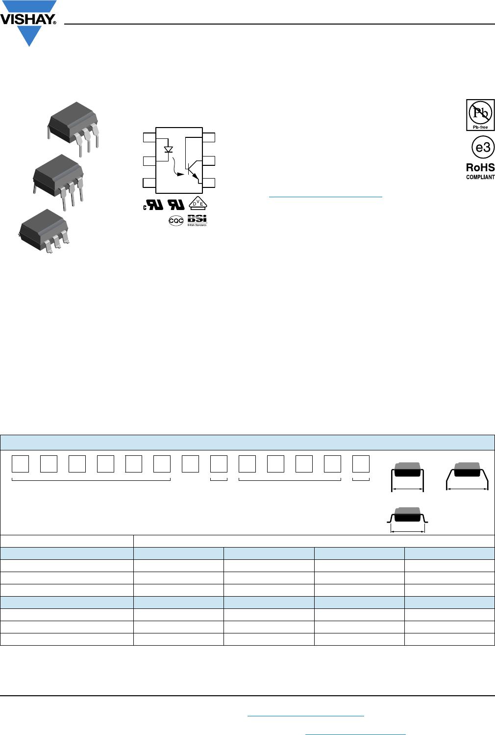
CNY117-2X006

CNY117
www.vishay.com
Vishay Semiconductors
Rev. 1.9, 08-Jan-14
1
Document Number: 83876
For technical questions, contact: optocoupleranswers@vishay.com
THIS DOCUMENT IS SUBJECT TO CHANGE WITHOUT NOTICE. THE PRODUCTS DESCRIBED HEREIN AND THIS DOCUMENT
ARE SUBJECT TO SPECIFIC DISCLAIMERS, SET FORTH AT www.vishay.com/doc?91000
Optocoupler, Phototransistor Output,
with Base Connection, 110 °C Rated
DESCRIPTION
The CNY117 is a 110 °C rated optocoupler consisting of a
gallium arsenide infrared emitting diode optically coupled to
a silicon planar phototransistor detector in a plastic plug-in
DIP-6 package.
The coupling device is suitable for signal transmission
between two electrically separated circuits. The potential
difference between the circuits to be coupled is not allowed
to exceed the maximum permissible reference voltages.
FEATURES
Operating temperature from -55 °C to +110 °C
Breakdown voltage, 5000 V
RMS
Long term stability
Industry standard dual-in-line package
Material categorization:
For definitions of compliance please see
www.vishay.com/doc?99912
APPLICATIONS
•AC adapter
•SMPS
•PLC
Factory automation
Game consoles
AGENCY APPROVALS
Safety application model number covering all products in
this datasheet is CNY117. This model number should be
used when consulting safety agency documents.
UL file no. E52744
cUL tested to CSA 22.2 bulletin 5A
DIN EN 60747-5-5 (VDE 0884-5), available with option 1
BSI: EN 60065, EN 60950-1
CQC GB8898-2011
Note
Additional options may be possible, please contact sales office.
1
2
3
6
5
4
B
C
E
A
C
NC
i179004-14
ORDERING INFORMATION
CNY117 - #X0##T
PART NUMBER CTR
BIN
PACKAGE OPTION TAPE
AND
REEL
AGENCY CERTIFIED/PACKAGE CTR (%)
UL, cUL, BSI 40 to 80 63 to 125 100 to 200 160 to 320
DIP-6 CNY117-1 CNY117-2 CNY117-3 CNY117-4
DIP-6, 400 mil, option 6 CNY117-1X006 CNY117-2X006 CNY117-3X006 CNY117-4X006
SMD-6, option 7 CNY117-1X007T CNY117-2X007T CNY117-3X007T CNY117-4X007T
VDE, UL, cUL, BSI 40 to 80 63 to 125 100 to 200 160 to 320
DIP-6 CNY117-1X001 CNY117-2X001 CNY117-3X001 CNY117-4X001
DIP-6, 400 mil, option 6 CNY117-1X016 CNY117-2X016 CNY117-3X016 CNY117-4X016
SMD-6, option 7 CNY117-1X017T CNY117-2X017T CNY117-3X017T CNY117-4X017T
7.62 mm 10.16 mm
> 8 mm
Option 7
Option 6
DIP-6
CNY117
www.vishay.com
Vishay Semiconductors
Rev. 1.9, 08-Jan-14
2
Document Number: 83876
For technical questions, contact: optocoupleranswers@vishay.com
THIS DOCUMENT IS SUBJECT TO CHANGE WITHOUT NOTICE. THE PRODUCTS DESCRIBED HEREIN AND THIS DOCUMENT
ARE SUBJECT TO SPECIFIC DISCLAIMERS, SET FORTH AT www.vishay.com/doc?91000
Notes
Stresses in excess of the absolute maximum ratings can cause permanent damage to the device. Functional operation of the device is not
implied at these or any other conditions in excess of those given in the operational sections of this document. Exposure to absolute
maximum ratings for extended periods of the time can adversely affect reliability.
(1)
Refer to reflow profile for soldering conditions for surface mounted devices (SMD). Refer to wave profile for soldering conditions for through
hole devices (DIP).
Note
Minimum and maximum values were tested requierements. Typical values are characteristics of the device and are the result of engineering
evaluations. Typical values are for information only and are not part of the testing requirements.
ABSOLUTE MAXIMUM RATINGS (T
amb
= 25 °C, unless otherwise specified)
PARAMETER TEST CONDITION SYMBOL VALUE UNIT
INPUT
Reverse voltage V
R
6.0 V
DC forward current I
F
60 mA
Surge forward current t 10 μs I
FSM
2.5 A
Power dissipation P
diss
100 mW
OUTPUT
Collector emitter breakdown voltage BV
CEO
70 V
Collector current I
C
50 mA
Collector peak current t
p
/T = 0.5, t
p
10 ms I
CM
100 mA
Output power dissipation P
diss
150 mW
COUPLER
Isolation test voltage
between emitter and detector referred to
standard climate 23/50 DIN 50014
t = 1 min V
ISO
5000 V
RMS
Storage temperature range T
stg
-55 to +150 °C
Ambient temperature range T
amb
-55 to +110 °C
Soldering temperature
(1)
2 mm from case, 10 s T
sld
260 °C
Total power dissipation P
diss
250 mW
ELECTRICAL CHARACTERISTICS (T
amb
= 25 °C, unless otherwise specified)
PARAMETER TEST CONDITION PART SYMBOL MIN. TYP. MAX. UNIT
INPUT
Forward voltage I
F
= 60 mA V
F
1.39 1.65 V
Breakdown voltage I
R
= 10 μA V
BR
6V
Reverse current V
R
= 6 V I
R
0.01 10 μA
Capacitance V
R
= 0 V, f = 1 MHz C
O
25 pF
OUTPUT
Collector emitter capacitance V
CE
= 5 V, f = 1 MHz C
CE
5.2 pF
Base collector capacitance V
CE
= 5 V, f = 1 MHz C
BC
6.5 pF
Emitter base capacitance V
CE
= 5 V, f = 1 MHz C
EB
7.5 pF
COUPLER
Collector emitter, saturation voltage I
F
= 10 mA, I
C
= 2.5 mA V
CEsat
0.25 0.4 V
Coupling capacitance C
C
0.6 pF
Collector emitter, leakage current V
CE
= 10 V
CNY117-1 I
CEO
2.0 50 nA
CNY117-2 I
CEO
2.0 50 nA
CNY117-3 I
CEO
5.0 100 nA
CNY117-4 I
CEO
5.0 100 nA
CNY117
www.vishay.com
Vishay Semiconductors
Rev. 1.9, 08-Jan-14
3
Document Number: 83876
For technical questions, contact: optocoupleranswers@vishay.com
THIS DOCUMENT IS SUBJECT TO CHANGE WITHOUT NOTICE. THE PRODUCTS DESCRIBED HEREIN AND THIS DOCUMENT
ARE SUBJECT TO SPECIFIC DISCLAIMERS, SET FORTH AT www.vishay.com/doc?91000
Note
Current transfer ratio I
C
/I
F
at V
CE
= 5.0 V, 25 °C and collector emitter leakage current by dash number.
CURRENT TRANSFER RATIO (T
amb
= 25 °C, unless otherwise specified)
PARAMETER TEST CONDITION PART SYMBOL MIN. TYP. MAX. UNIT
Current transfer ratio
I
F
= 10 mA
CNY117-1 CTR 40 80 %
CNY117-2 CTR 63 125 %
CNY117-3 CTR 100 200 %
CNY117-4 CTR 160 320 %
I
F
= 1.0 mA
CNY117-1 CTR 13 30 %
CNY117-2 CTR 22 45 %
CNY117-3 CTR 34 70 %
CNY117-4 CTR 56 90 %
SWITCHING CHARACTERISTICS (T
amb
= 25 °C, unless otherwise specified)
PARAMETER TEST CONDITION PART SYMBOL MIN. TYP. MAX. UNIT
LINEAR OPERATION (without saturation)
Turn-on time
I
F
= 10 mA, V
CC
= 5.0 V,
R
L
= 75 Ω
t
on
3.0 μs
Rise time
I
F
= 10 mA, V
CC
= 5.0 V,
R
L
= 75 Ω
t
r
2.0 μs
Turn-off time
I
F
= 10 mA, V
CC
= 5.0 V,
R
L
= 75 Ω
t
off
2.3 μs
Fall time
I
F
= 10 mA, V
CC
= 5.0 V,
R
L
= 75 Ω
t
f
2.0 μs
Cut-off frequency
I
F
= 10 mA, V
CC
= 5.0 V,
R
L
= 75 Ω
f
CO
110 kHz
SWITCHING OPERATION (with saturation)
Turn-on time
I
F
= 20 mA CNY117-1 t
on
3.0 μs
I
F
= 10 mA
CNY117-2 t
on
4.2 μs
CNY117-3 t
on
4.2 μs
I
F
= 5.0 mA CNY117-4 t
on
6.0 μs
Rise time
I
F
= 20 mA CNY117-1 t
r
2.0 μs
I
F
= 10 mA
CNY117-2 t
r
3.0 μs
CNY117-3 t
r
3.0 μs
I
F
= 5.0 mA CNY117-4 t
r
4.6 μs
Turn-off time
I
F
= 20 mA CNY117-1 t
off
18 μs
I
F
= 10 mA
CNY117-2 t
off
23 μs
CNY117-3 t
off
23 μs
I
F
= 5.0 mA CNY117-4 t
off
25 μs
Fall time
I
F
= 20 mA CNY117-1 t
f
11 μs
I
F
= 10 mA
CNY117-2 t
f
14 μs
CNY117-3 t
f
14 μs
I
F
= 5.0 mA CNY117-4 t
f
15 μs

CNY117-2X006

Mfr. #:
Manufacturer:
Vishay Semiconductors
Description:
Transistor Output Optocouplers Phototransistor Out Single CTR 63-125%
Lifecycle:
New from this manufacturer.
Delivery:
DHL FedEx Ups TNT EMS
Payment:
T/T Paypal Visa MoneyGram Western Union