www.vishay.com
6
Document Number: 64814
S09-0872-Rev. A, 18-May-09
Vishay Siliconix
Si7145DP
New Product
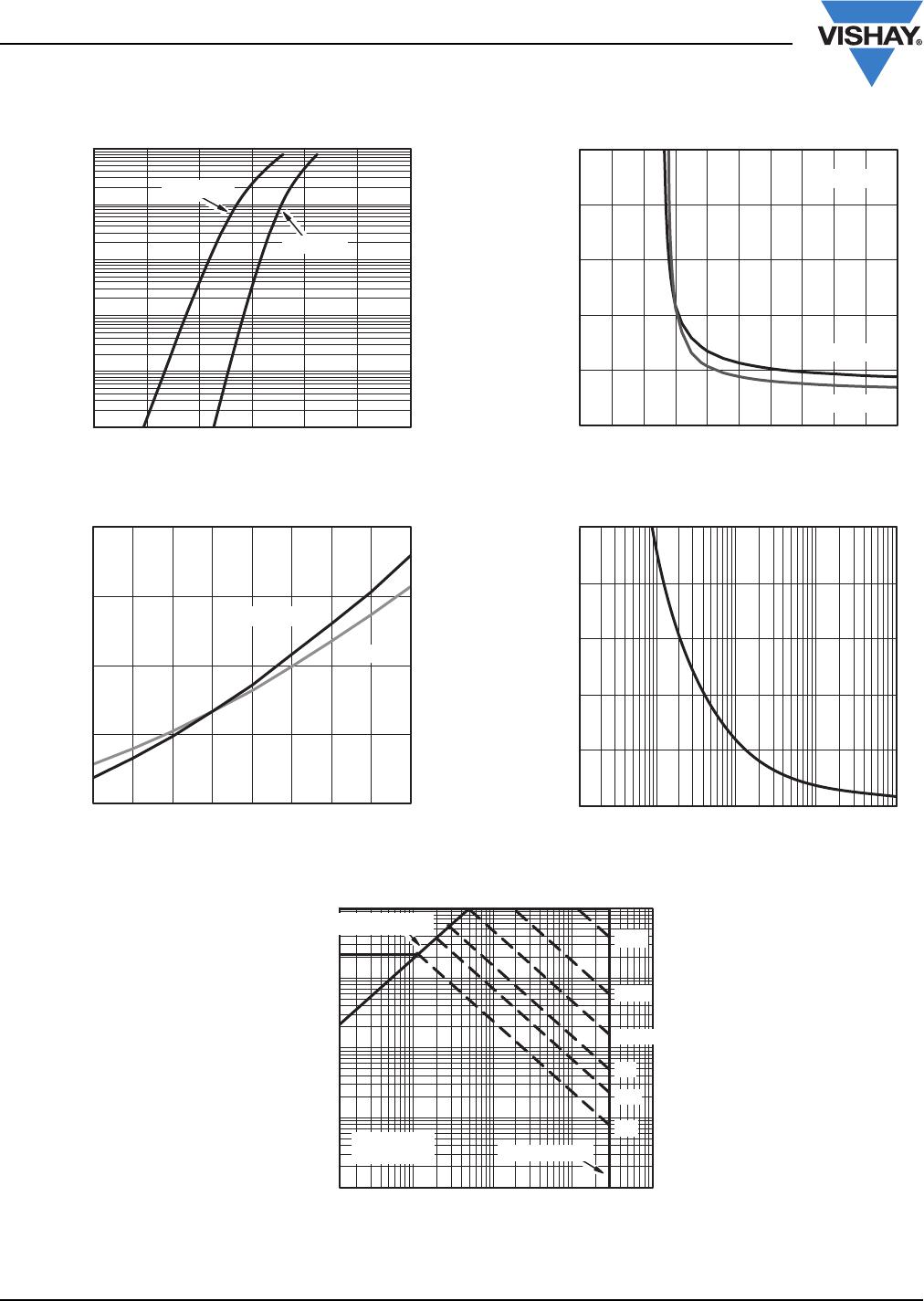
TYPICAL CHARACTERISTICS 25 °C, unless otherwise noted
Vishay Siliconix maintains worldwide manufacturing capability. Products may be manufactured at one of several qualified locations. Reliability data for Silicon
Technology and Package Reliability represent a composite of all qualified locations. For related documents such as package/tape drawings, part marking, and
reliability data, see www.vishay.com/ppg?64814
.
Normalized Thermal Transient Impedance, Junction-to-Ambient
10
-3
10
-2
1
10
100010
-1
10
-4
100
0.2
0.1
Square WavePulse Duration (s)
Normalized Effective Transient
Thermal Impedance
1
0.1
0.01
t
1
t
2
Notes:
P
DM
1. Duty Cycle, D =
2. Per Unit Base = R
thJA
= 54 °C/W
3. T
JM
-T
A
=P
DM
Z
thJA
(t)
t
1
t
2
4. Surface Mounted
Duty Cycle = 0.5
Single Pulse
0.02
0.05
Normalized Thermal Transient Impedance, Junction-to-Case
10
-3
10
-2
01110
-1
10
-4
0.2
0.1
Duty Cycle = 0.5
Square WavePulse Duration (s)
Normalized Effective Transient
Thermal Impedance
1
0.1
0.01
0.05
Single Pulse
0.02