2
LTC1560-1
sn15601 15601fs
ABSOLUTE MAXIMUM RATINGS
W
WW
U
PACKAGE/ORDER INFORMATION
W
U
U
Total Supply Voltage (V
+
to V
–
) ............................. 12V
Power Dissipation............................................. 400mW
Burn-In Voltage ................................................... ±5.5V
Operating Temperature Range
LTC1560-1C ........................................... 0°C to 70°C
LTC1560-1I ....................................... –40°C to 85°C
Maximum Junction Temperature ......................... 150°C
Storage Temperature Range ................. –65°C to 150°C
Lead Temperature (Soldering, 10 sec).................. 300°C
ORDER PART
NUMBER
LTC1560-1CS8
LTC1560-1IS8
The ● denotes specifications which apply over the full operating
temperature range.
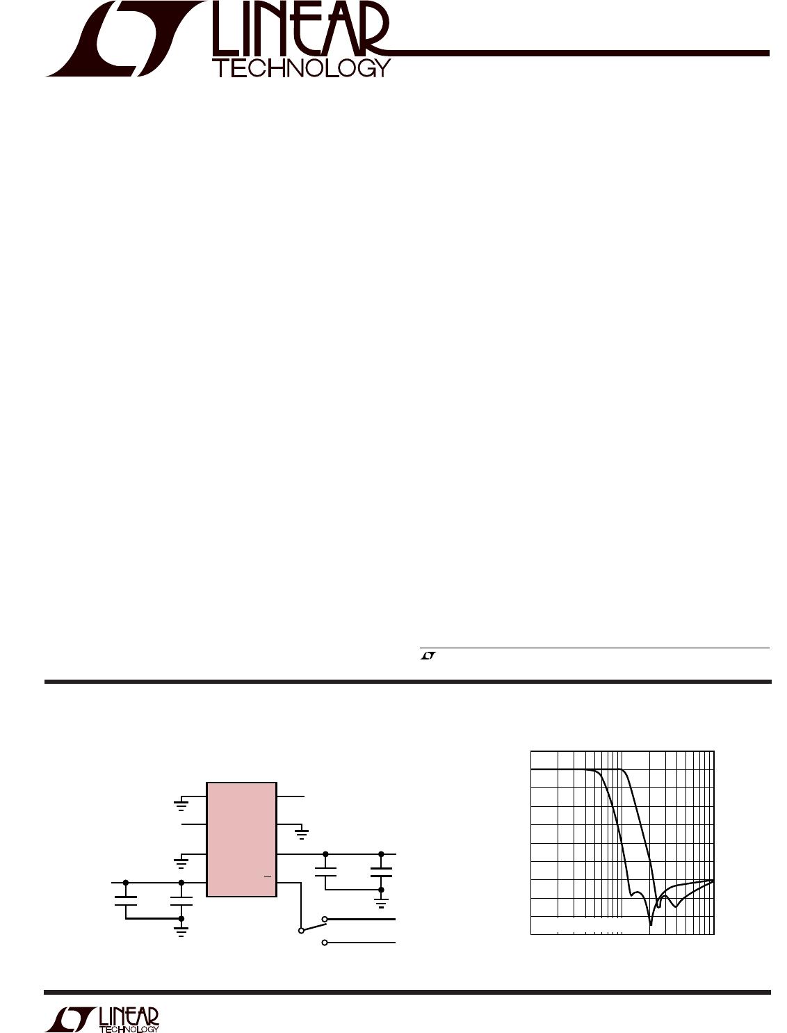
Note 1: To properly measure high frequency characteristics of the filter, a
noninverting output buffer is recommended as shown on the demo board
connection diagram, Figure 2. A small resistor (e.g. 100Ω) can also be
used instead of the buffer to isolate any high capacitive load (C
L
> 10pF)
from the filter output.
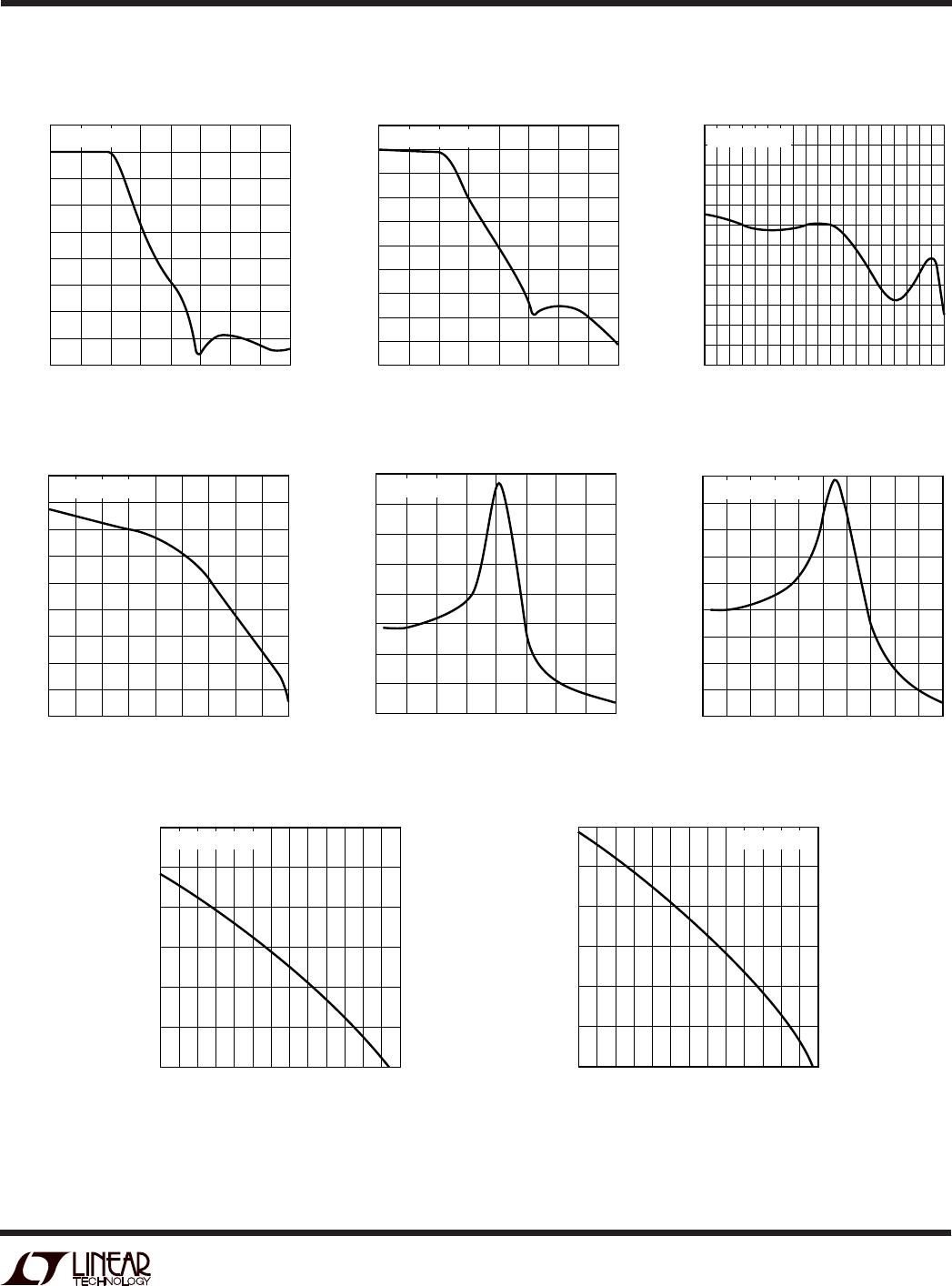
Note 2: The stopband gain at 2.44MHz is guaranteed by design.
PARAMETER CONDITIONS MIN TYP MAX UNITS
Operating Supply Voltage Range ±4.5 ±5.0 ±5.5 V
Passband Gain (f
CUTOFF
= 1MHz) V
IN
= 0.5V
RMS
,f
IN
= 20kHz 0.17 dB
f
IN
= 100kHz ● –0.3 0.18 0.6 dB
f
IN
= 300kHz 0.08 dB
f
IN
= 550kHz (Gain Relative to 100kHz) ● –0.35 0.05 0.3 dB
f
IN
= 850kHz (Gain Relative to 100kHz) ● –0.8 – 0.3 0 dB
f
IN
= 950kHz (Gain Relative to 100kHz) ● –3.0 0.6 0.5 dB
f
IN
= f
CUTOFF
= 1MHz (Gain Relative to 100kHz) ● –5.0 –1.0 1.0 dB
Transition Band Gain (Note 1) V
IN
= 0.5V
RMS
,f
IN
= 1.4MHz ● –24 –18 dB
f
IN
= 1.9MHz –42 dB
f
IN
= 2.0MHz –51 dB
Stopband Gain (f
CUTOFF
= 1MHz) (Note 2) f
IN
= 2.44MHz ● –70 –65 dB
f
IN
= 3.0MHz –68 dB
f
IN
= 6.0MHz –66.1 dB
Passband Gain (f
CUTOFF
= 500kHz) f
IN
= 100kHz, Pin 5 = 5V 0.14 dB
f
IN
= f
CUTOFF
= 500kHz ● –4 –1.6 0.5 dB
f
IN
= 1.4MHz –45 dB
Output Voltage Swing R
L
= 5k ±2.20 ±3V
R
L
= 5k ● ±1.75 V
Output DC Offset (V
OS
) ±250 mV
Power Supply Current (I
S
) ● 22 29 mA
Power Supply Current in Shutdown Mode Pin 7 at 5V 1 mA
Total Output Noise V
IN
(Pin 2) Tied to Ground, f
CUTOFF
= 1MHz, BW = 2MHz 350 µV
RMS
V
IN
(Pin 2) Tied to Ground, f
CUTOFF
= 0.5MHz, BW = 1MHz 322 µV
RMS
Total Harmonic Distortion (THD) V
IN
= 1V
RMS
, f
IN
= 200kHz, f
CUTOFF
= 1MHz, BW = 1MHz –63 dB
f
IN
= 300kHz, f
CUTOFF
= 1MHz, BW = 1MHz –61 dB
f
IN
= 1MHz, f
CUTOFF
= 1MHz, BW = 2MHz –62 dB
f
IN
= 300kHz, f
CUTOFF
= 0.5MHz, BW = 1MHz –62 dB
f
IN
= 500kHz, f
CUTOFF
= 0.5MHz, BW = 1MHz –63 dB
Input Resistance (R
IN
) ● 6810 kΩ
ELECTRICAL CHARACTERISTICS
V
S
= ±5V, T
A
= 25°C, Pin 5 = –5V (f
CUTOFF
= 1MHz), Pin 7 = 0V unless otherwise specified.
S8 PART MARKING
15601
15601I
Consult factory for Military grade parts.
T
JMAX
= 150°C, θ
JA
= 125°C/ W
1
2
3
4
8
7
6
5
TOP VIEW
V
OUT
SHDN
V
+
GND
V
IN
GND
V
–
S8 PACKAGE
8-LEAD PLASTIC SO
0.5f
C/
f
C