© Semiconductor Components Industries, LLC, 2014
July, 2014 − Rev. 11
1 Publication Order Number:
MC14538B/D
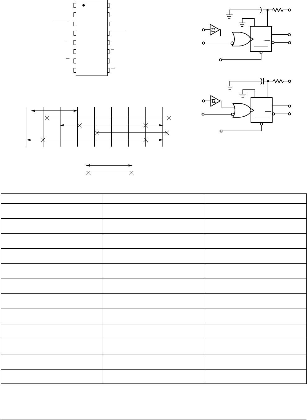
MC14538B
Dual Precision
Retriggerable/Resettable
Monostable Multivibrator
The MC14538B is a dual, retriggerable, resettable monostable
multivibrator. It may be triggered from either edge of an input pulse,
and produces an accurate output pulse over a wide range of widths, the
duration and accuracy of which are determined by the external timing
components, C
X
and R
X
. Output Pulse Width T = R
X
@ C
X
(secs)
R
X
= W
C
X
= Farads
Features
• Unlimited Rise and Fall Time Allowed on the A Trigger Input
• Pulse Width Range = 10 ms to 10 s
• Latched Trigger Inputs
• Separate Latched Reset Inputs
• 3.0 Vdc to 18 Vdc Operational Limits
• Triggerable from Positive (A Input) or Negative−Going Edge (B−Input)
• Capable of Driving Two Low−Power TTL Loads or One Low−Power
Schottky TTL Load Over the Rated Temperature Range
• Pin−for−pin Compatible with MC14528B and CD4528B (CD4098)
• Use the MC54/74HC4538A for Pulse Widths Less Than 10 ms with
Supplies Up to 6 V
• NLV Prefix for Automotive and Other Applications Requiring
Unique Site and Control Change Requirements; AEC−Q100
Qualified and PPAP Capable
• These Devices are Pb−Free and are RoHS Compliant
MAXIMUM RATINGS (Voltages Referenced to V
SS
)
Symbol Parameter Value Unit
V
DD
DC Supply Voltage Range −0.5 to +18.0 V
V
in
, V
out
Input or Output Voltage Range
(DC or Transient)
−0.5 to V
DD
+ 0.5 V
I
in
, I
out
Input or Output Current
(DC or Transient) per Pin
±10 mA
P
D
Power Dissipation, per Package
(Note 1)
500 mW
T
A
Operating Temperature Range −55 to +125 °C
T
stg
Storage Temperature Range −65 to +150 °C
T
L
Lead Temperature
(8−Second Soldering)
260 °C
Stresses exceeding those listed in the Maximum Ratings table may damage the
device. If any of these limits are exceeded, device functionality should not be
assumed, damage may occur and reliability may be affected.
1. Temperature Derating: “D/DW” Packages: –7.0 mW/_C From 65_C To 125_C
This device contains protection circuitry to guard against damage due to high
static voltages or electric fields. However, precautions must be taken to avoid
applications of any voltage higher than maximum rated voltages to this
high−impedance circuit. For proper operation, V
in
and V
out
should be constrained
to the range V
SS
≤ (V
in
or V
out
) ≤ V
DD
.
Unused inputs must always be tied to an appropriate logic voltage level
(e.g., either V
SS
or V
DD
). Unused outputs must be left open.
http://onsemi.com
MARKING DIAGRAMS
SOIC−16WB
DW SUFFIX
CASE 751G
A = Assembly Location
WL, L = Wafer Lot
YY, Y = Year
WW, W = Work Week
G or G = Pb−Free Indicator
SOEIAJ−16
F SUFFIX
CASE 966
MC14538B
ALYWG
See detailed ordering and shipping information in the package
dimensions section on page 2 of this data sheet.
ORDERING INFORMATION
1
16
14538BG
AWLYYWW
16
1
SOIC−16
D SUFFIX
CASE 751B
TSSOP−16
DT SUFFIX
CASE 948F
14538BG
AWLYWW
1
16
14
538B
ALYWG
G
1
16
(Note: Microdot may be in either location)
SOIC−16WB
SOEIAJ−16
SOIC−16
TSSOP−16