10
LTC1334
SWITCHI G WAVEFOR S
U
W
1.5V
3V
0V
DE
f = 1MHz: t
r
10ns: t
f
10ns
1.5V
Y, Z
V
OL
5V
t
ZL
t
LZ
0.5V
OUTPUT NORMALLY LOW
0V
LTC1334 • F07
2.3V
2.3V
t
ZH
V
OH
OUTPUT NORMALLY HIGH
t
HZ
0.5V
Z, Y
0V
V
OD2
B – A
f = 1MHz: t
r
10ns: t
f
10ns
1.5V
R
V
OL
V
OH
LTC1334 • F08
t
PLH
t
PHL
INPUT
–V
OD2
OUTPUT
0V
1.5V
3V
D
Y, Z
–V
O
V
O
LTC1334 • F09
t
PHL
t
PLH
0V
0V
0V
1.5V
1.5V
V
IH
A, B
R
V
OL
V
OH
LTC1334 • F10
t
PHL
t
PLH
V
IL
2.4V
0.8V
1.3V
1.7V
Figure 7. RS485 Driver Enable and Disable Times
Figure 8. RS485 Receiver Propagation Delays
Figure 10. RS232 Receiver Propagation Delays
Figure 9. RS232 Driver Propagation Delays
11
LTC1334
U
S
A
O
PP
L
IC
AT
I
WU
U
I FOR ATIO
Basic Theory of Operation
The LTC1334 has two interface ports. Each port may be
configured as a pair of single-ended RS232 transceivers
or as a differential RS485 transceiver by forcing the
port’s selection input to a low or high, respectively. The
LTC1334 provides two RS232 drivers and two RS232
receivers or one RS485 driver and one RS485 receiver
per port. All the interface drivers feature three-state
outputs. Interface outputs are forced into high imped-
ance when the driver is disabled, in the shutdown mode
or with the power off.
All the interface driver outputs are fault-protected by a
current limiting and thermal shutdown circuit. The ther-
mal shutdown circuit disables both the RS232 and RS485
driver outputs when the die temperature reaches 150°C.
The thermal shutdown circuit reenables the drivers when
the die temperature cools to 130°C.
In RS485 mode, shutdown mode or with the power off, the
input resistance of the receiver is 24k. The input resistance
drops to 5k in RS232 mode.
A logic low at the ON/OFF pin shuts down the device and
forces all the outputs into a high impedance state. A logic
high enables the device. An internal 4µA current source to
V
CC
pulls the ON/OFF pin high if it is left open.
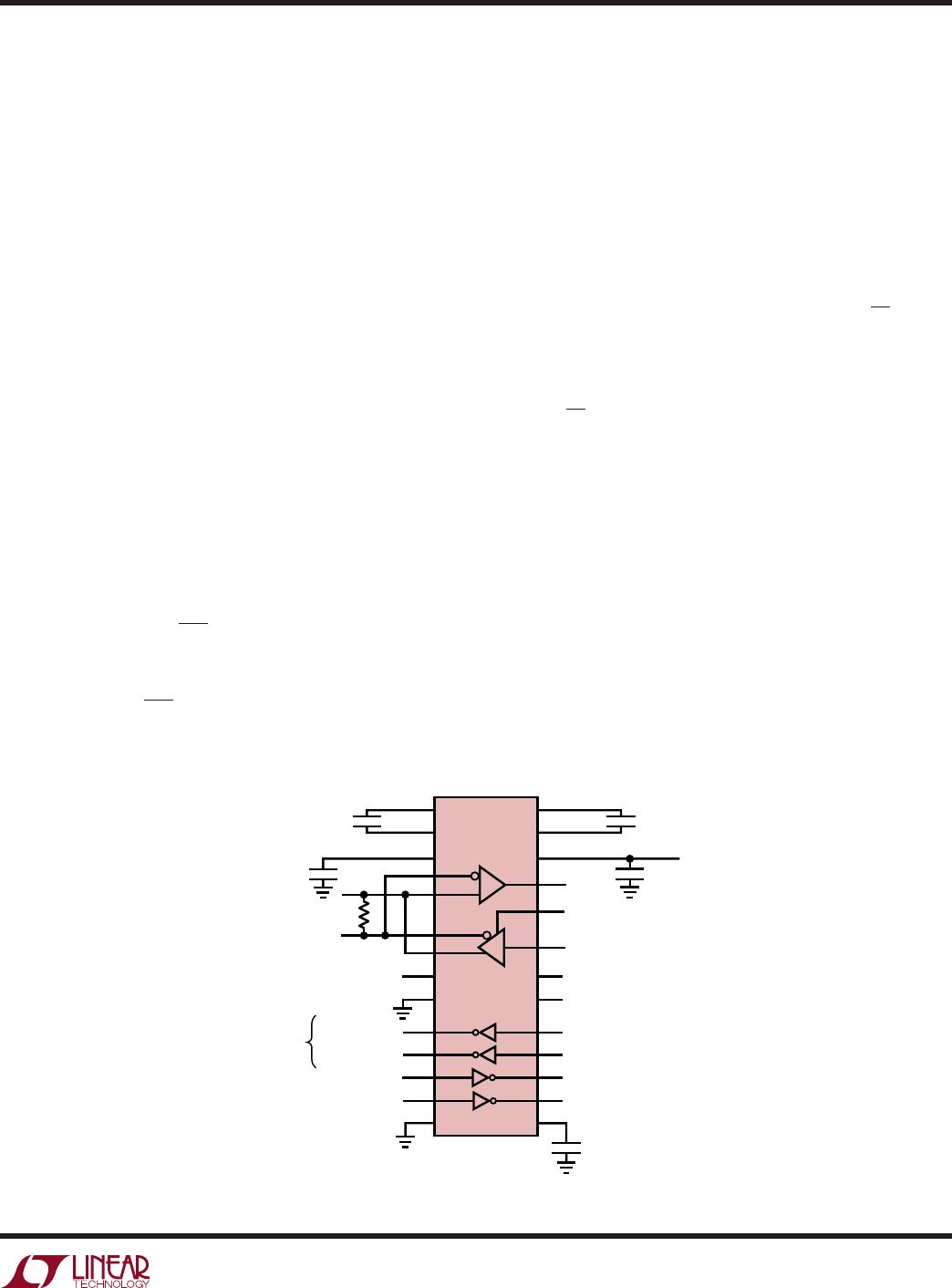
Figure 11. RS232/RS485 Interfaces
1
28
V
CC
5V
LTC1334 • F11
120
12
21
LTC1334
RX OUT
18
5V
13
10
11
9
8
14
17
16
RS485 I/O
RS232 DR OUT
19
5V
20
15
V
EE
5V
±5V INTO
3k LOAD
5
4
27
26
24
RX OUT
6
RS232 RX IN
23
2
3
RX OUT
7
DR IN
DR ENABLE
DR IN
DR IN
22
RS232 DR OUT
RS232 RX IN
V
DD
C1
C2
0.1µF
0.1µF
0.1µF0.1µF
0.1µF
In RS485 mode, an internal 4µA current source pulls the
driver enable pin high if left open. The RS485 receiver has
a 4µA current source at the noninverting input. If both the
RS485 receiver inputs are open, the output goes to a high
state. Both the current sources are disabled in the RS232
mode. The receiver output B is inactive in RS485 mode
and has a 50k pull-up resistor to provide a known output
state in this mode.
A loopback mode enables internal connections from driver
outputs to receiver inputs for self-test when the LB pin has
a low logic state. The driver outputs are not isolated from
the external loads. This allows transmitter verification
under the loaded condition. An internal 4µA current source
pulls the LB pin high if left open and disables the loopback
configuration.
RS232/RS485 Applications
The LTC1334 can support both RS232 and RS485 levels
with a single 5V supply as shown in Figure 11.
Multiprotocol Applications
The LTC1334 is well-suited for software controlled inter-
face mode selection. Each port has a selection pin as
shown in Figure 12. The single-ended transceivers sup-
port both RS232 and EIA562 levels. The differential trans-
ceivers support both RS485 and RS422.
12
LTC1334
U
S
A
O
PP
L
IC
AT
I
WU
U
I FOR ATIO
Figure 12. Multiprotocol Interface
with Optional, Switchable Terminations
326
25
RX OUT
24
RX OUT
22
DR IN
8
SEL1
23
21
DR IN/ENABLE
LB
V
CC
5V
LTC1334 • F12
LTC1334
28
C2C1
2
1
27
V
EE
V
DD
4
INPUT A
K1A
K1B
120
5
INPUT B
6
OUTPUT A
7
OUTPUT B
13
INPUT A
12
INPUT B
11
OUTPUT A
10
14
OUTPUT B
PORT 1
INTERFACE
20
16
ON/OFF
RX OUT
17
RX OUT
19
DR IN
9
SEL2
18
15
DR IN/ENABLE
PORT 2
INTERFACE
AROMAT CORP (800) 276-6289
ZETEX (516) 543-7100
*
**
0.1µF
0.1µF 0.1µF
0.1µF0.1µF
120
K2A
120
K2B
120
TERM1
360k
FMMT619**
K1*
TX2A-5V
7.5k
TERM2
360k
FMMT619**
K2*
TX2A-5V
7.5k
5V
5V
Figure 13. Typical Connection for RS232/EIA562 Interface
1/2 LTC1334 1/2 LTC1334
LTC1334 • F13
19
18
17
16
9
DR IN
DR IN
RX OUT
RX OUT
4
5
6
7
11
10
13
12
24
25
22
23
8
RX OUT
RX OUT
DR IN
DR IN
RS232/
EIA562
INTERFACE
LINES
Each receiver in the LTC1334 is designed to present one
unit load (5k nominal for RS232 and 12k minimum for
RS485) to the cable. Some RS485 and RS422 applications
call for terminations, but these are only necessary at two
nodes in the system and they must be disconnected when
operating in the RS232 mode. A relay is the simplest, low-
est cost method of switching terminations. In Figure 12
TERM1 and TERM2 select 120 terminations as needed.
If terminations are needed in all RS485/RS422 applica-
tions, no extra control signals are required; simply con-
nect TERM1 and TERM2 to SEL1 and SEL2.
Typical Applications
A typical RS232/EIA562 interface application is shown in
Figure 13 with the LTC1334.
A typical connection for a RS485 transceiver is shown in
Figure 14. A twisted pair of wires connects up to 32 drivers
and receivers for half duplex multipoint data transmission.
The wires must be terminated at both ends with resistors
equal to the wire’s characteristic impedance. An optional
shield around the twisted pair helps to reduce unwanted
noise and should be connected to ground at only one end.
Figure 14. Typical Connection for RS485 Interface
5V
4
1/2 LTC1334
1/2
LTC1334
1/2 LTC1334
LTC1334 F14
RX OUT
DR ENABLE
DR IN
5V
120
5
6
7
24
23
22
8
13
12
11
10
9
RX OUT
18
5V
DR ENABLE
76 54
22
DR IN RX OUT
DR ENABLE
23 24 8
17
DR IN
19
120

LTC1334CG#PBF

Mfr. #:
Manufacturer:
Analog Devices Inc.
Description:
RS-232 Interface IC +5V Multi Protocol Transceiver
Lifecycle:
New from this manufacturer.
Delivery:
DHL FedEx Ups TNT EMS
Payment:
T/T Paypal Visa MoneyGram Western Union