July 2005 1 MIC4423/4424/4425
MIC4423/4424/4425 Micrel, Inc.
INA
OUTA
INVERTING
NONINVERTING
0.1mA
0.6mA
2kΩ
INB
OUTB
INVERTING
NONINVERTING
0.1mA
0.6mA
2kΩ
V
S
GND
MIC4423/4424/4425
Dual 3A-Peak Low-Side MOSFET Driver
Bipolar/CMOS/DMOS Process
Features
• Reliable, low-power bipolar/CMOS/DMOS construction
• Latch-up protected to >500mA reverse current
• Logic input withstands swing to –5V
• High 3A-peak output current
• Wide 4.5V to 18V operating range
• Drives 1800pF capacitance in 25ns
• Short <40ns typical delay time
• Delay times consistent with in supply voltage change
• Matched rise and fall times
• TTL logic input independent of supply voltage
• Low equivalent 6pF input capacitance
• Low supply current
3.5mA with logic-1 input
350µA with logic-0 input
• Low 3.5Ω typical output impedance
• Output voltage swings within 25mV of ground or V
S
.
• ‘426/7/8-, ‘1426/7/8-, ‘4426/7/8-compatible pinout
• Inverting, noninverting, and differential configurations
General Description
The MIC4423/4424/4425 family are highly reliable BiCMOS/
DMOS buffer/driver/MOSFET drivers. They are higher out-
put current versions of the MIC4426/4427/4428, which are
improved versions of the MIC426/427/428. All three families
are pin-compatible. The MIC4423/4424/4425 drivers are ca-
pable of giving reliable service in more demanding electrical
environments than their predecessors. They will not latch
under any conditions within their power and voltage ratings.
They can survive up to 5V of noise spiking, of either polarity,
on the ground pin. They can accept, without either damage
or logic upset, up to half an amp of reverse current (either
polarity) forced back into their outputs.
The MIC4423/4424/4425 series drivers are easier to use, more
flexible in operation, and more forgiving than other CMOS
or bipolar drivers currently available. Their BiCMOS/DMOS
construction dissipates minimum power and provides rail-to-
rail voltage swings.
Primarily intended for driving power MOSFETs, the
MIC4423/4424/4425 drivers are suitable for driving other loads
(capacitive, resistive, or inductive) which require low-imped
-
ance, high peak currents, and fast switching times. Heavily
loaded clock lines, coaxial cables, or piezoelectric transducers
are some examples. The only known limitation on loading is
that total power dissipated in the driver must be kept within
the maximum power dissipation limits of the package.
Note: See MIC4123/4124/4125 for high power and narrow
pulse applications.
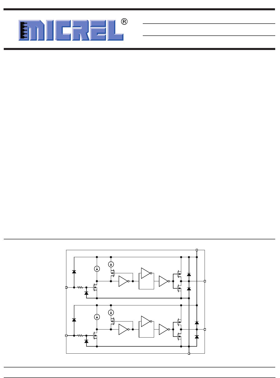
Functional Diagram
Integrated Component Count:
4 Resistors
4 Capacitors
52 Transistors
Ground Unused Inputs
Micrel, Inc. • 2180 Fortune Drive • San Jose, CA 95131 • USA • tel + 1 (408) 944-0800 • fax + 1 (408) 474-1000 • http://www.micrel.com

