ISL6730A, ISL6730B, ISL6730C, ISL6730D
14
FN8258.1
August 8, 2013
The MOSFET, SPP20N60C3 is selected.
The switching loss of the MOSFET consists of three parts: the
turn-on loss, the turn-off loss and the diode reverse recovery loss.
From the MOSFET datasheet, the typical switching losses curves
are provided.
When R
G
= 3.6Ω, I
D
= 6A, E
ON
= 0.015mJ, E
OFF
= 0.007mJ.
The switching loss due to transition is calculated:
The diode reverse recovery incurs additional power loss on the
MOSFET. This loss can be estimated as:
This loss is also related the di/dt during the MOSFET turn-on. The
di/dt can be found out from the MOSFET datasheet. At
R
G
= 3.6Ω, the turn-on di/dt is 4000A/µs. From the Typical
Reverse Recovery Charge curve at T
J
= +125°C, the
Q
RR
= 220nC when I
F
= 3.5A.
THE TOTAL LOSS ON THE MOSFET
OUTPUT CAPACITOR SELECTION
The output capacitor, C
OUT
, is required to hold the output above
300V during one line cycle. For capacitors with 20% tolerance,
the tolerance should be taken into consideration. Thus, the
output capacitance should be greater than:
Calculate the ripple RMS current through the capacitor:
Select the proper capacitor according to the hold time and ripple
RMS current requirement. The actual capacitance is 270µF.
It is important to make sure the output peak-to-peak ripple is
less than the minimum OVP threshold as specified in the
“Electrical Specifications” table on page 6. The ESR at 2 times of
the line frequency of the capacitor is found in the capacitor
datasheet. The ESR of the output capacitor is 770mΩ at 100Hz.
The minimum OVP threshold is 103% of the nominal output
value. The maximum output peak to peak ripple should be less
than 6% of the nominal value, which is 23.4V
P-P
.
CURRENT SENSING RESISTORS
Please refer to Equation 4 for calculation of the current sensing
resistor R
CS
.
While a large R
CS
renders better current sensing accuracy, larger
R
CS
also incurs higher power dissipation. Select R
CS
from
available standard value resistors to determine the sense
resistor.
The maximum power dissipation on the R
CS
occurs at low line
and full load condition. The maximum power dissipation is
calculated:
The resistor, R
SEN
sets the overcurrent protection limit. From
Equation 3, R
SEN
should be greater than:
Where |x| stands for the ABS(x) function.
Select R
SEN
from available standard value resistors, the selected
R
SEN
is 3.16kΩ.
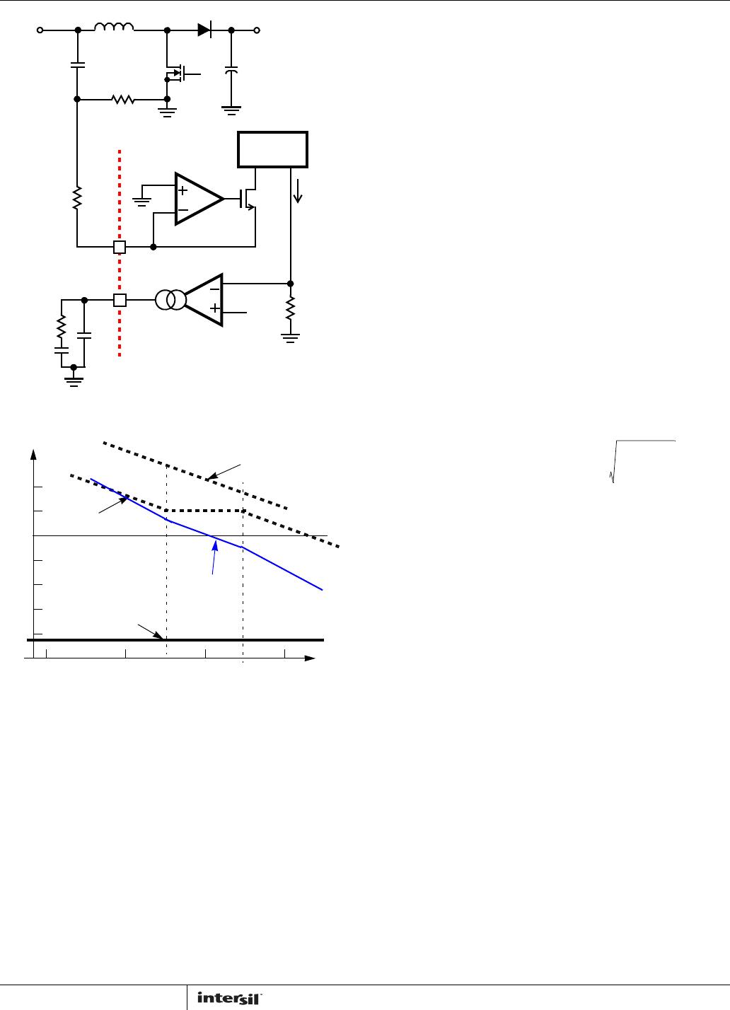
CURRENT LOOP COMPENSATION
The input current shaping is achieved by comparing the sensed
current signal to the sensed input voltage signal. The current
error amplifier (Gmi), together with the current compensation
network, adjusts the duty cycle so that the inductor current
traces the sensed rectified voltage. Thus, unity power factor is
achieved.
The compensation network consists of the Trans-Conductance
error amplifier (Gmi) and the impedance network (Z
ICOMP).
The
goal of the compensation network is to provide a closed loop
transfer function with the sufficient 0dB crossing frequency
(f
0dB
) and adequate phase margin. Phase margin is the
difference between the open loop phase at f
0dB
and 180°. The
following equations relate the compensation network’s poles,
zeros and gain to the components (R
ic
, C
ic
and C
ip
) in Figure 15.
P
COND
I
DS max()
2
R
DS on()
•=
(EQ. 27)
P
COND
3.3A
2
0.3Ω• 3.27W==
(EQ. 28)
P
SW
E
ON
E
OFF
+()F•
sw
=
(EQ. 29)
P
SW
0.015mJ 0.007mJ+()62kHz• 1.36W==
(EQ. 30)
P
RR
Q
RR
V
OUT
• F•
sw
=
(EQ. 31)
P
RR
220nC 390V 62• kHz• 5.32W==
(EQ. 32)
P
COND
P
SW
P+
RR
+ 3.27W 1.36W 5.32W++ 9.95W==
(EQ. 33)
C
OUT
2T
HOLD
P⋅⋅
OMAX
V
OUT
2
V
HOLD
2
–
----------------------------------------------------
1
10.2–
-----------------
⋅≥
(EQ. 34)
C
OUT
2 20ms 300W⋅⋅
390()
2
300V()
2
–
----------------------------------------------
1.25 242μF=⋅≥
(EQ. 35)
I
CORMS max()
I
OUT max()
82
3π
-----------
V
OUT
V
RMSmin
--------------------------
• 1–=
(EQ. 36)
I
CORMS max()
0.77A
82
3π
-----------
390V
85V
--------------
• 1– 1.635A==
(EQ. 37)
V
Opp
I
OUT max()
4πf
line
C
OUT
ESR⋅⋅()
2
1+
4πf
line
()C
OUT
0.8⋅⋅
-------------------------------------------------------------------------------
⋅=
(EQ. 38)
V
Opp
0.77A
4π 50Hz 270μF0.77Ω⋅⋅ ⋅()
2
1+
4π 50Hz⋅()270μF0.8⋅⋅
--------------------------------------------------------------------------------------------
⋅ 6.6V==
(EQ. 39)
R
CS
120mV 265V 0.92⋅⋅
2300W⋅
-------------------------------------------------------
≥ 0.069Ω=
(EQ. 40)
P
RCSMAX
I
INMAX
2
R•
CS
=
(EQ. 42)
P
RCSMAX
3.88A
2
0.068Ω• 1.023W==
(EQ. 43)
R
SEN
R
CS
I
LPeak
10.25+()••
20.5I
OC
•
--------------------------------------------------------------------
≥
(EQ. 44)
R
SEN
0.068Ω 6.6A 1.25••
290μA•
--------------------------------------------------------
≥ 3.117kΩ=
(EQ. 45)