LTC1043
6
1043fa
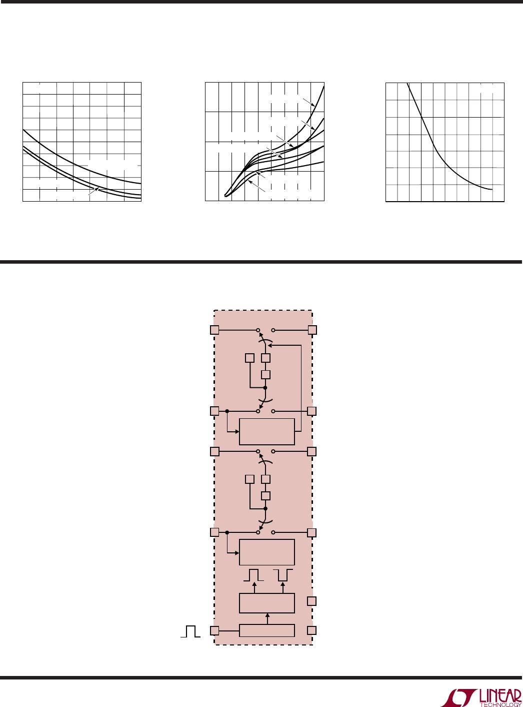
Figure 2. CMRR vs Sampling Frequency
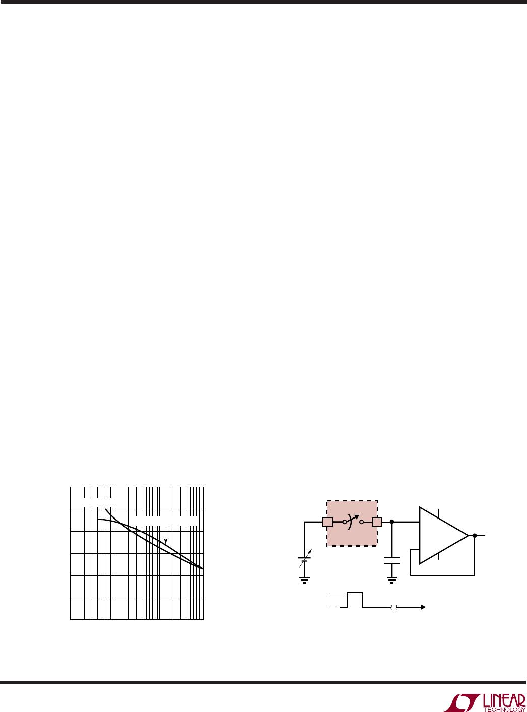
Figure 3
APPLICATIO S I FOR ATIO
WUUU
f
OSC
(Hz)
100
20
CMRR (dB)
100
120
140
1k 10k 100k
LTC1043 • AI02
80
60
40
C
S
= C
H
= 1µF
C
S
= 1µF, C
ZH
= 0.1µF
LTC1043 • AI03
1/8 LTC1043
6
V
OUT
V
IN
V
+
SAMPLE
HOLD TO PIN 16
0V
1000pF
5V
–5V
–
+
2
1/2 LTC1013
shorting Pins 7 and 13 and by observing, with a precision
DVM, the change of the voltage across C
H
with respect to
an input CM voltage variation. During the sampling and
holding mode, charges are being transferred and minute
voltage transients will appear across the holding capaci-
tor. Although the R
ON
on the switches is low enough to
allow fast settling, as the sampling frequency increases,
the rate of charge transfer increases and the average
voltage measured with a DVM across it will increase
proportionally; this causes the CMRR of the sampled data
system, as seen by a “continuous” instrument (DVM), to
decrease (Figure 2).
Switch Charge Injection
Figure 3 shows one out of the eight switches of the
LTC1043, configured as a basic sample-and-hold circuit.
When the switch opens, a ‘‘hold step’’ is observed and its
magnitude depends on the value of the input voltage.
Figure 4 shows charge injected into the hold capacitor. For
instance, a 2pCb of charge injected into a 0.01µF capacitor
causes a 200µV hold step. As shown in Figure 4, there is
a predictable and repeatable charge injection cancellation
when the input voltage is close to half the supply voltage
of the LTC1043. This is a unique feature of this product,
containing charge-balanced switches fabricated with a
self-aligning gate CMOS process. Any switch of the
LTC1043, when powered with symmetrical dual supplies,
will sample-and-hold small signals around ground with-
out any significant error.
Shielding the Sampling Capacitor for Very High CMRR
Internal or external parasitic capacitors from the C
+
pin(s)
to ground affect the CMRR of the LTC1043 (Figure 1).
The common mode error due to the internal junction
capacitances of the C
+
Pin(s) 2 and 11 is cancelled through
internal circuitry. The C
+
pin, therefore, should be used as
the top plate of the sampling capacitor. The interpin
capacitance between pin 2 and dummy Pin 1 (11 and 10)
appears in parallel with the sampling capacitor so it does
not degrade the CMRR. A shield placed underneath
the sampling capacitor and connected to either Pin 1 or 3
helps to boost the CMRR in excess of 120dB (Figure 5).
Excessive external parasitic capacitance between the C
–
pins and ground indirectly degrades CMRR; this becomes
visible especially when the LTC1043 is used with clock
frequencies above 2kHz. Because of this, if a shield is
used, the parasitic capacitance between the shield and
circuit ground should be minimized.
It is recommended that the outer plate of the sampling
capacitor be connected to the C
–
pin(s).
Input Pins, SCR Sensitivity
An internal 60Ω resistor is connected in series with the
input of the switches (Pins 5, 6, 7, 8, 13, 14, 15, 18) and
it is included in the R
ON
specification. When the input
voltage exceeds the power supply by a diode drop, current
will flow into the input pin(s). The LTC1043 will not latch
until the input current reaches 2mA–3mA. The device will