10
LTC1693
corresponding to MOSFET’s V
GS
value (V
CC
in this case)
can be readily obtained from the manafacturer’s Q
GS
vs
V
GS
curves:
Load Capacitive Power (MOS) = (V
CC
)(Q
G
)(f)
Transition state power losses are due to both AC currents
required to charge and discharge the drivers’ internal
nodal capacitances and cross-conduction currents in the
internal gates.
UVLO and Thermal Shutdown
The LTC1693’s UVLO detector disables the input buffer
and pulls the output pin to ground if V
CC
< 4V. The output
remains off from V
CC
= 1V to V
CC
= 4V. This ensures that
during start-up or improper supply voltage values, the
LTC1693 will keep the output power MOSFET off.
The LTC1693 also has a thermal detector that similarly
disables the input buffer and grounds the output pin if
junction temperature exceeds 145°C. The thermal shut-
down circuit has 20°C of hysteresis. This thermal limit
helps to shut down the system should a fault condition
occur.
Input Voltage Range
LTC1693’s input pin is a high impedance node and essen-
tially draws neligible input current. This simplifies the
input drive circuitry required for the input.
The LTC1693 typically has 1.2V of hysteresis between its
low and high input thresholds. This increases the driver’s
robustness against any ground bounce noises. However,
care should still be taken to keep this pin from any noise
pickup, especially in high frequency switching
applications.
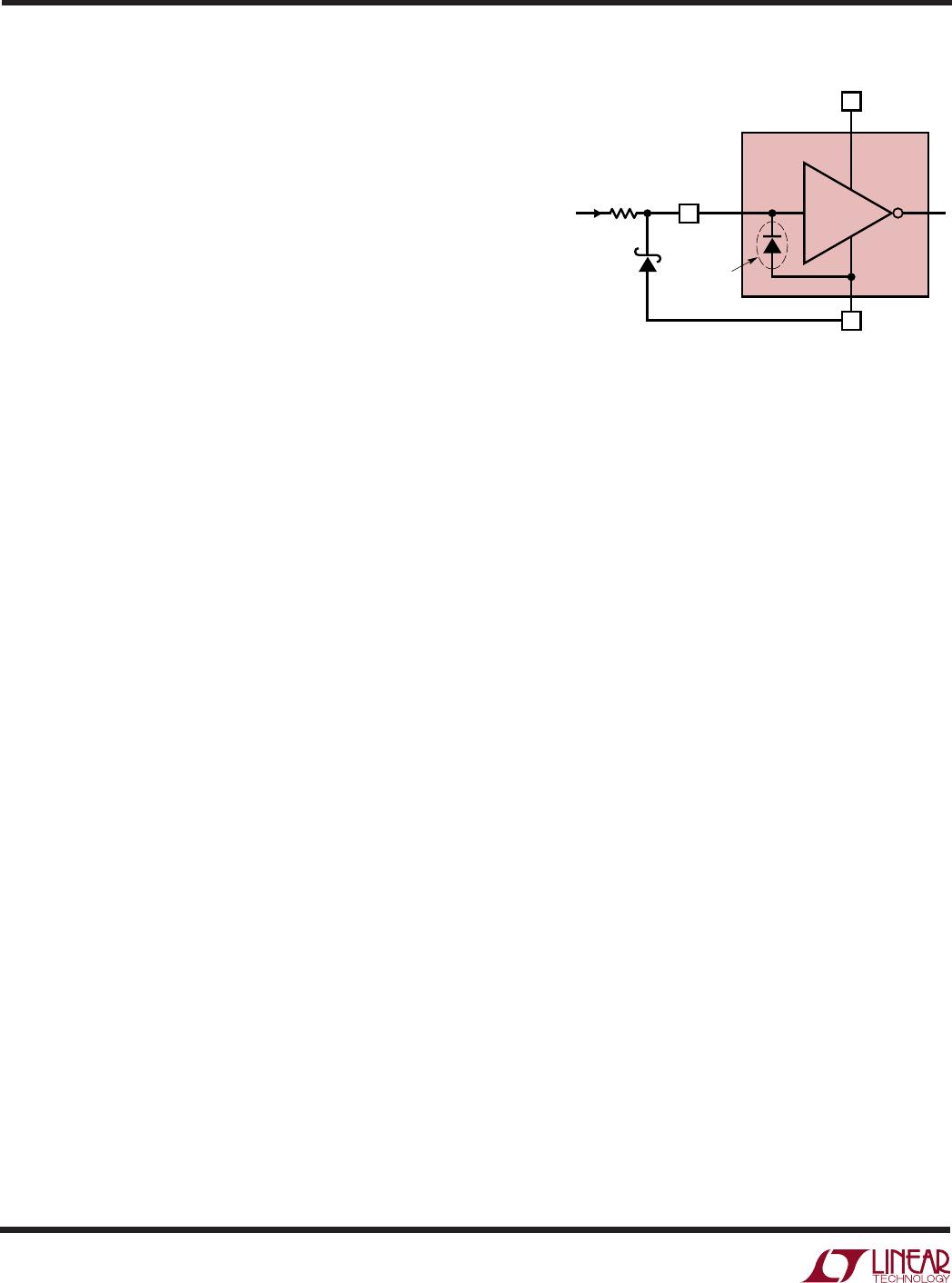
In applications where the input signal swings below the
GND pin potential, the input pin voltage must be clamped
to prevent the LTC1693’s parastic substrate diode from
turning on. This can be accomplished by connecting a
series current limiting resistor R1 and a shunting Schottky
diode D1 to the input pin (Figure 4). R1 ranges from 100Ω
to 470Ω while D1 can be a BAT54 or 1N5818/9.
V
CC
IN
R1
D1
GND
LTC1693
INPUT SIGNAL
GOING BEL0W
GND PIN
POTENTIAL
PARASITIC
SUBSTRATE
DIODE
1693 F04
Bypassing and Grounding
LTC1693 requires proper V
CC
bypassing and grounding due
to its high speed switching (ns) and large AC currents (A).
Careless component placement and PCB trace routing may
cause excessive ringing and under/overshoot.
To obtain the optimum performance from the LTC1693:
A. Mount the bypass capacitors as close as possible to the
V
CC
and GND pins. The leads should be shortened as
much as possible to reduce lead inductance. It is
recommended to have a 0.1µF ceramic in parallel with
a low ESR 4.7µF bypass capacitor.
For high voltage switching in an inductive environment,
ensure that the bypass capacitors’ V
MAX
ratings are
high enough to prevent breakdown. This is especially
important for floating driver applications.
B. Use a low inductance, low impedance ground plane to
reduce any ground drop and stray capacitance. Re-
member that the LTC1693 switches 1.5A peak currents
and any significant ground drop will degrade signal
integrity.
C. Plan the ground routing carefully. Know where the large
load switching current is coming from and going to.
Maintain separate ground return paths for the input pin
and output pin. Terminate these two ground traces only
at the GND pin of the driver (STAR network).
D. Keep the copper trace between the driver output pin and
the load short and wide.
Figure 4
APPLICATIONS INFORMATION
WUU
U