© Semiconductor Components Industries, LLC, 2013
May, 2017 − Rev. 13
1 Publication Order Number:
MBRA160T3/D
MBRA160, NRVBA160
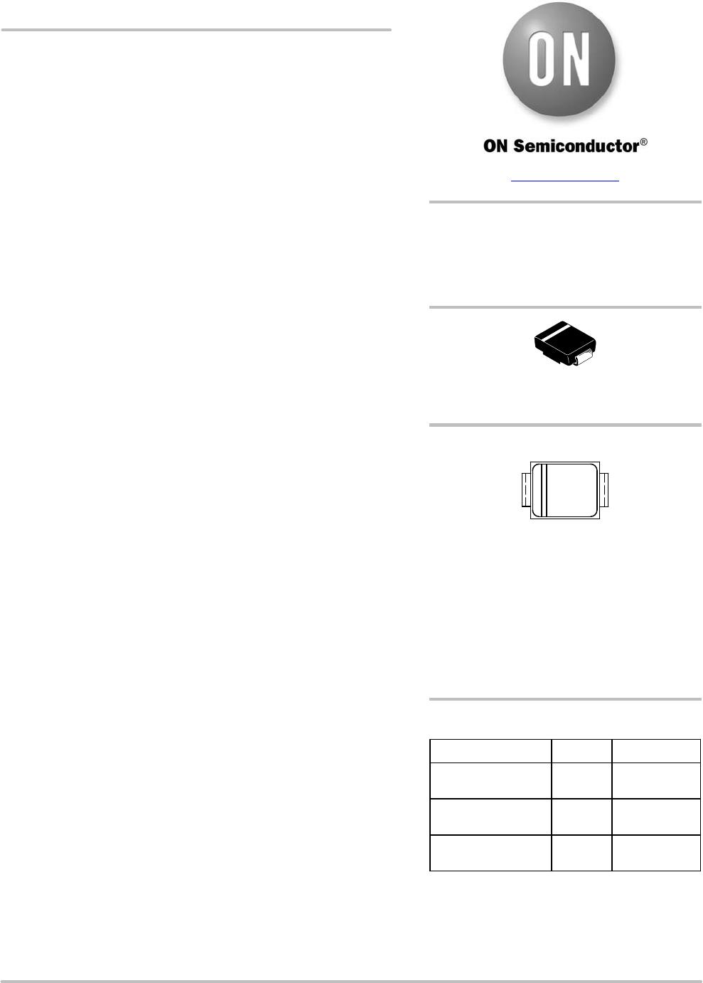
Surface Mount
Schottky Power Rectifier
SMA Power Surface Mount Package
This device employs the Schottky Barrier principle in a large area
metal−to−silicon power diode. State of the art geometry features
epitaxial construction with oxide passivation and metal overlay
contact. Ideally suited for low voltage, high frequency rectification, or
as free wheeling and polarity diodes in surface mount applications
where compact size and weight are critical to the system.
Features
• Small Compact Surface Mountable Package with J−Bent Leads
• Rectangular Package for Automated Handling
• Highly Stable Oxide Passivated Junction
• Very Low Forward Voltage Drop
• Guard−ring for Stress Protection
• NRVBA Prefix for Automotive and Other Applications Requiring
Unique Site and Control Change Requirements; AEC−Q101
Qualified and PPAP Capable*
• These Devices are Pb−Free, Halogen Free/BFR Free and are RoHS
Compliant
Mechanical Characteristics:
• Case: Epoxy, Molded
• Weight: 70 mg (Approximately)
• Finish: All External Surfaces Corrosion Resistant and Terminal
Leads are Readily Solderable
• Lead and Mounting Surface Temperature for Soldering Purposes:
260°C Max. for 10 Seconds
• Shipped in 12 mm tape, 5000 units per 13 inch reel
• Polarity: Cathode Lead Indicated by Polarity Band
• ESD Ratings:
♦ Machine Model = C
♦ Human Body Model = 3B
Device Package Shipping
†
ORDERING INFORMATION
SCHOTTKY BARRIER
RECTIFIER
1.0 AMPERES
60 VOLTS
MARKING DIAGRAM
SMA
CASE 403D
www.onsemi.com
MBRA160T3G SMA
(Pb−Free)
5,000 /
Tape & Reel
B16
AYWW
G
B16 = Specific Device Code
A = Assembly Location**
Y = Year
WW = Work Week
G = Pb−Free Package
NRVBA160T3G* SMA
(Pb−Free)
5,000 /
Tape & Reel
†For information on tape and reel specifications,
including part orientation and tape sizes, please
refer to our Tape and Reel Packaging Specification
Brochure, BRD8011/D.
**The Assembly Location code (A) is front sid
optional. In cases where the Assembly Location
stamped in the package bottom (molding ejecter pin
the front side assembly code may be blank.
(Note: Microdot may be in either location)
NRVBA160T3G−VF01 SMA
(Pb−Free)
5,000 /
Tape & Reel