BYG21KHM3_A/H

BYG21K-M3/HM3, BYG21M-M3/HM3
www.vishay.com
Vishay General Semiconductor
Revision: 23-Feb-16
1
Document Number: 89476
For technical questions within your region: DiodesAmericas@vishay.com
, DiodesAsia@vishay.com, DiodesEurope@vishay.com
THIS DOCUMENT IS SUBJECT TO CHANGE WITHOUT NOTICE. THE PRODUCTS DESCRIBED HEREIN AND THIS DOCUMENT
ARE SUBJECT TO SPECIFIC DISCLAIMERS, SET FORTH AT www.vishay.com/doc?91000
Fast Avalanche SMD Rectifier
FEATURES
Low profile package
Ideal for automated placement
Glass passivated pellet chip junction
Low reverse current
Soft recovery characteristic
Fast reverse recovery time
Meets MSL level 1, per J-STD-020, LF maximum peak
of 260 °C
AEC-Q101 qualified
Material categorization: for definitions of compliance
please see www.vishay.com/doc?99912
TYPICAL APPLICATIONS
For use in fast switching rectification of power supply,
inverters, converters, and freewheeling diodes for
consumer, automotive, and telecommunication.
MECHANICAL DATA
Case: DO-214AC (SMA)
Molding compound meets UL 94 V-0 flammability rating
Base P/N-M3 - halogen-free, RoHS-compliant, and
commercial grade
Base P/NHM3 - halogen-free, RoHS-compliant, and
AEC-Q101 qualified
Terminals: Matte tin plated leads, solderable per
J-STD-002 and JESD 22-B102
M3 suffix meets JESD 201 class 2 whisker test, HM3 suffix
meets JESD 201 class 2 whisker test
Polarity: Color band denotes the cathode end
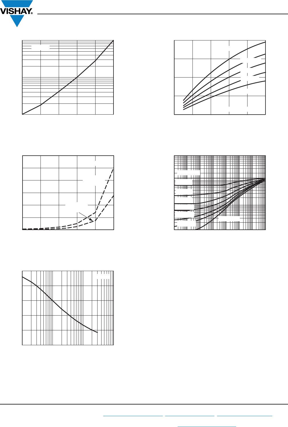
PRIMARY CHARACTERISTICS
I
F(AV)
1.5 A
V
RRM
800 V, 1000 V
I
FSM
30 A
I
R
1.0 μA
V
F
1.6 V
t
rr
120 ns
E
R
20 mJ
T
J
max. 150 °C
Package DO-214AC (SMA)
Diode variation Single die
DO-214AC (SMA)
MAXIMUM RATINGS (T
A
= 25 °C unless otherwise noted)
PARAMETER SYMBOL BYG21K BYG21M UNIT
Device marking code BYG21K BYG21M
Maximum repetitive peak reverse voltage V
RRM
800 1000 V
Average forward current I
F(AV)
1.5 A
Peak forward surge current 10 ms single half sine-wave
superimposed on rated load
I
FSM
30 A
Pulse energy in avalanche mode, non repetitive
(inductive load switch off) I
(BR)R
= 1 A, T
J
= 25 °C
E
R
20 mJ
Operating junction and storage temperature range T
J
, T
STG
-55 to +150 °C
BYG21K-M3/HM3, BYG21M-M3/HM3
www.vishay.com
Vishay General Semiconductor
Revision: 23-Feb-16
2
Document Number: 89476
For technical questions within your region: DiodesAmericas@vishay.com
, DiodesAsia@vishay.com, DiodesEurope@vishay.com
THIS DOCUMENT IS SUBJECT TO CHANGE WITHOUT NOTICE. THE PRODUCTS DESCRIBED HEREIN AND THIS DOCUMENT
ARE SUBJECT TO SPECIFIC DISCLAIMERS, SET FORTH AT www.vishay.com/doc?91000
Note
(1)
Pulse test: 300 μs pulse width, 1 % duty cycle
Notes
(1)
Mounted on epoxy-glass hard tissue
(2)
Mounted on epoxy-glass hard tissue, 50 mm
2
35 μm Cu
(3)
Mounted on Al-oxide-ceramic (Al
2
O
3
), 50 mm
2
35 μm Cu
Note
(1)
AEC-Q101 qualified
RATINGS AND CHARACTERISTICS CURVES (T
A
= 25 °C unless otherwise noted)
Fig. 1 - Forward Current vs. Forward Voltage Fig. 2 - Max. Average Forward Current vs. Ambient Temperature
ELECTRICAL CHARACTERISTICS (T
A
= 25 °C unless otherwise noted)
PARAMETER TEST CONDITIONS SYMBOL BYG21K BYG21M UNIT
Maximum instantaneous
forward voltage
I
F
= 1 A
T
J
= 25 °C V
F
(1)
1.5
V
I
F
= 1.5 A 1.6
Maximum reverse current V
R
= V
RRM
T
J
= 25 °C
I
R
1
μA
T
J
= 100 °C 10
Maximum reverse
recovery time
I
F
= 0.5 A, I
R
= 1.0 A,
I
rr
= 0.25 A
t
rr
120 ns
THERMAL CHARACTERISTICS (T
A
= 25 °C unless otherwise noted)
PARAMETER SYMBOL BYG21K BYG21M UNIT
Typical thermal resistance, junction to lead, T
L
= const. R
JL
25 °C/W
Typical thermal resistance, junction to ambient
R
JA
(1)
150
°C/WR
JA
(2)
125
R
JA
(3)
100
ORDERING INFORMATION (Example)
PREFERRED P/N UNIT WEIGHT (g) PREFERRED PACKAGE CODE BASE QUANTITY DELIVERY MODE
BYG21K-M3/TR 0.064 TR 1800 7" diameter plastic tape and reel
BYG21K-M3/TR3 0.064 TR3 7500 13" diameter plastic tape and reel
BYG21KHM3/TR
(1)
0.064 TR 1800 7" diameter plastic tape and reel
BYG21KHM3/TR3
(1)
0.064 TR3 7500 13" diameter plastic tape and reel
0.001
0.01
0.1
1
10
0 0.5 1.0 1.5 2.0 2.5 3.0 3.5
Forward Voltage (V)
Forward Current (A)
T
J
= 150 °C
T
J
= 25 °C
0.0
0.2
0.4
0.6
0.8
1.0
1.2
1.4
1.6
Ambient Temperature (°C)
Average Forward Current (A)
1007550250 125 150
V
R
= V
RRM
Half Sine-Wave
R
θJA
= 25 K/W
R
θJA
= 125 K/W
R
θJA
= 150 K/W
BYG21K-M3/HM3, BYG21M-M3/HM3
www.vishay.com
Vishay General Semiconductor
Revision: 23-Feb-16
3
Document Number: 89476
For technical questions within your region: DiodesAmericas@vishay.com
, DiodesAsia@vishay.com, DiodesEurope@vishay.com
THIS DOCUMENT IS SUBJECT TO CHANGE WITHOUT NOTICE. THE PRODUCTS DESCRIBED HEREIN AND THIS DOCUMENT
ARE SUBJECT TO SPECIFIC DISCLAIMERS, SET FORTH AT www.vishay.com/doc?91000
Fig. 3 - Reverse Current vs. Junction Temperature
Fig. 4 - Max. Reverse Power Dissipation vs. Junction Temperature
Fig. 5 - Diode Capacitance vs. Reverse Voltage
Fig. 6 - Max. Reverse Recovery Charge vs. Forward Current
Fig. 7 - Thermal Response
1
10
100
25 50 75 100 125 150
Reverse Current (µA)
Junction Temperat
u
re (°C)
V
R
= V
RRM
0
20
40
60
80
100
120
25 50 75 100 125 150
Reverse Power Dissipation (mW)
Junction Temperature (°C)
V
R
= V
RRM
P
R
- Limit
at 100 % V
R
P
R
- Limit
at 80 % V
R
0
5
10
15
20
25
0.1 1 10 100
f = 1 MHz
Reverse Voltage (V)
Diode Capacitance (pF)
T
A
= 125 °C
0
50
100
150
200
0 0.2 0.4 0.6 0.8 1.0
Reverse Recovery Charge (nC)
Forward Current (A)
T
A
= 100 °C
T
A
= 25 °C
T
A
= 75 °C
T
A
= 50 °C
I
R
= 0.5 A, i
R
= 0.125 A
1
10
100
1000
Thermal Resistance for Pulse Cond. (K/W)
Pulse Length (s)
10
-5
10
-4
10
-3
10
-2
10
-1
10
0
10
1
10
2
Single Pulse
125 K/W DC
t
p
/T = 0.5
t
p
/T = 0.2
t
p
/T = 0.1
t
p
/T = 0.05
t
p
/T = 0.02
t
p
/T = 0.01

BYG21KHM3_A/H

Mfr. #:
Manufacturer:
Vishay Semiconductors
Description:
Rectifiers 1.5A,800V,120nS AVAL AEC-Q101 Qualified
Lifecycle:
New from this manufacturer.
Delivery:
DHL FedEx Ups TNT EMS
Payment:
T/T Paypal Visa MoneyGram Western Union