LTC3109
6
3109fb
For more information www.linear.com/LTC3109
LDO Step Load Response Enable Input and V
OUT2
Running on Storage Capacitor
pin FuncTions
(QFN/SSOP)
VSTORE (Pin 1/Pin 3): Output for the Storage Capacitor or
Battery. A large storage capacitor may be connected from
this pin to GND for powering the system in the event the
input voltage is lost. It will be charged up to the maximum
VAUX clamp voltage. If not used, this pin should be left
open or tied to VAUX.
VAUX (Pin 2/Pin 4): Output of the Internal Rectifier Cir
-
cuit and V
CC
for the IC. Bypass VAUX with at least 1µF of
capacitance to ground. An active shunt regulator clamps
VAUX to 5.25V (typical).
V
OUT
(Pin 3/Pin 5): Main Output of the Converter. The
voltage at this pin is regulated to the voltage selected by
VS1 and VS2 (see Table 1). Connect this pin to a reservoir
capacitor or to a rechargeable battery. Any high current
pulse loads must be fed by the reservoir capacitor on
this pin.
V
OUT2
(Pin 4/ Pin 6): Switched Output of the Converter.
Connect this pin to a switched load. This output is open
until V
OUT_EN
is driven high, then it is connected to V
OUT
through a 1Ω PMOS switch. If not used, this pin should
be left open or tied to V
OUT
.
V
OUT2_EN
(Pin 5/Pin 7): Enable Input for V
OUT2
. V
OUT2
will be enabled when this pin is driven high. There is an
internal 5M pull-down resistor on this pin. If not used,
this pin can be left open or grounded.
PGOOD (Pin 6/Pin 8): Power Good Output. When V
OUT
is within 7.5% of its programmed value, this pin will be
pulled up to the LDO voltage through a 1M resistor. If
V
OUT
drops 9% below its programmed value PGOOD will
go low. This pin can sink up to 100µA.
VLDO (Pin 7/Pin 9): Output of the 2.2V LDO. Connect a
2.2µF or larger ceramic capacitor from this pin to GND.
If not used, this pin should be tied to VAUX.
GND (Pins 8, 11, 16, Exposed Pad Pin 21/Pins 10, 13,
18): Ground Pins. Connect these pins directly to the ground
plane. The exposed pad serves as a ground connection and
as a means of conducting heat away from the die.
VS2 (Pin 20/Pin 2): V
OUT
Select Pin 2. Connect this
pin to ground or VAUX to program the output voltage
(see Table 1).
VS1 (Pin 19/Pin 1): V
OUT
Select Pin 1. Connect this
pin to ground or VAUX to program the output voltage
(see Table 1).
Table 1. Regulated Output Voltage Using Pins VS1 and VS2
VS2 VS1 V
OUT
GND GND 2.35V
GND VAUX 3.3V
VAUX GND 4.1V
VAUX VAUX 5.0V
Typical perForMance characTerisTics
T
A
= 25°C, unless otherwise noted.
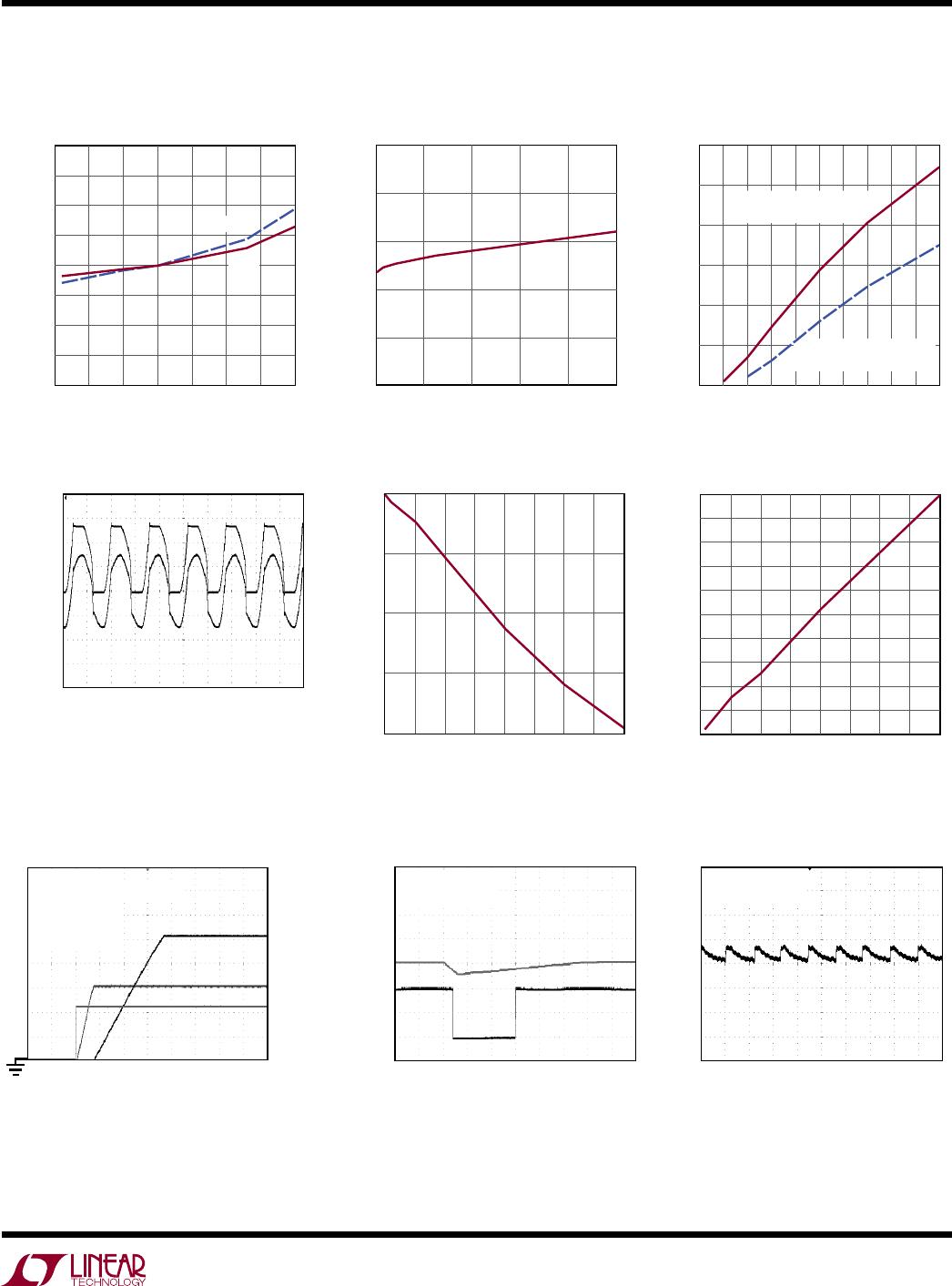
V
LDO
20mV/DIV
I
LDO
5mA/DIV
200µs/DIV
3109 G15
0mA TO 3mA LOAD STEP
C
= 2.2µF
1ms/DIV
3109 G16
CH2
V
OUT2
1V/DIV
CH1
V
OUT2_EN
1V/DIV
10mA LOAD ON V
OUT2
C
= 220µF
5SEC/DIV
3109 G17
CH2, V
OUT
1V/DIV
CH1, V
IN
50mV/DIV
CH3
VSTORE
1V/DIV
CH4, V
LDO
1V/DIV
C
STORE
= 470µF
V
OUT
LOAD = 100µA