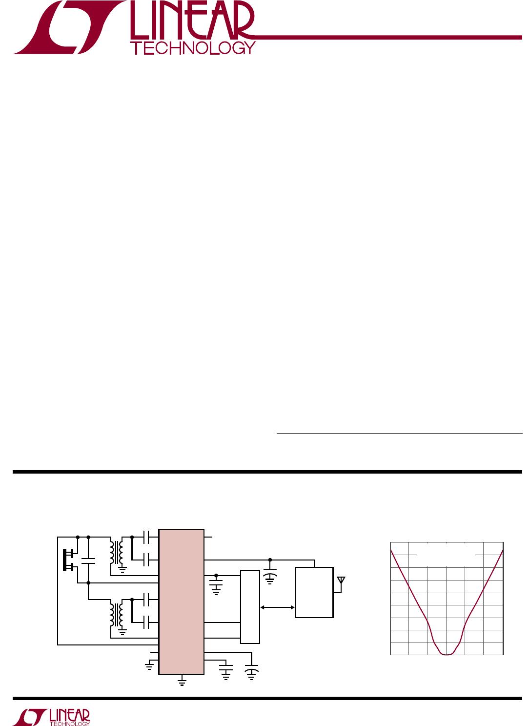
LTC3109
3
3109fb
For more information www.linear.com/LTC3109
elecTrical characTerisTics
Note 1: Stresses beyond those listed under Absolute Maximum Ratings
may cause permanent damage to the device. Exposure to any Absolute
Maximum Rating condition for extended periods may affect device
reliability and lifetime.
Note 2: The LTC3109 is tested under pulsed load conditions such that
T
J
≈ T
A
. The LTC3109E is guaranteed to meet specifications from
The l denotes the specifications which apply over the full operating
junction temperature range, otherwise specifications are for T
A
= 25°C (Note 2). VAUX = 5V unless otherwise noted.
PARAMETER CONDITIONS MIN TYP MAX UNITS
Minimum Start-Up Voltage Using 1:100 Transformer Turns Ratio, VAUX = 0V ±30 ±50 mV
No-Load Input Current Using 1:100 Transformer Turns Ratios,
V
IN
= 30mV, V
OUT2_EN
= 0V, All Outputs Charged
and in Regulation
6 mA
Input Voltage Range Using 1:100 Transformer Turns Ratios
l
V
STARTUP
±500 mV
Output Voltage VS1 = VS2 = GND
VS1 = VAUX, VS2 = GND
VS1 = GND, VS2 = VAUX
VS1 = VS2 = VAUX
l
l
l
l
2.30
3.234
4.018
4.875
2.350
3.300
4.100
5.000
2.40
3.366
4.182
5.10
V
V
V
V
VAUX Quiescent Current No Load, All Outputs Charged 7 10 µA
VAUX Clamp Voltage Current Into VAUX = 5mA
l
5.0 5.25 5.55 V
V
OUT
Quiescent Current V
OUT
= 3.3V, V
OUT2_EN
= 0V 0.2 µA
V
OUT
Current Limit V
OUT
= 0V
l
6 15 26 mA
N-Channel MOSFET On-Resistance C2B = C2A = 5V (Note 3) Measured from V
INA
or
SWA, V
INB
or SWB to GND
0.35 Ω
LDO Output Voltage 0.5mA Load On V
LDO
l
2.134 2.2 2.30 V
LDO Load Regulation For 0mA to 2mA Load 0.5 1 %
LDO Line Regulation For V
AUX
from 2.5V to 5V 0.05 0.2 %
LDO Dropout Voltage I
LDO
= 2mA
l
100 200 mV
LDO Current Limit V
LDO
= 0V
l
5 12 mA
VSTORE Leakage Current VSTORE = 5V 0.1 0.3 µA
VSTORE Current Limit VSTORE = 0V
l
6 15 26 mA
V
OUT2
Leakage Current V
OUT2
= 0V, V
OUT2_EN
= 0V 50 nA
VS1, VS2 Threshold Voltage
l
0.4 0.85 1.2 V
VS1, VS2 Input Current V
S1
= V
S2
= 5V 1 50 nA
PGOOD Threshold (Rising) Measured Relative to the V
OUT
Voltage –7.5 %
PGOOD Threshold (Falling) Measured Relative to the V
OUT
Voltage –9 %
PGOOD V
OL
Sink Current = 100µA 0.12 0.3 V
PGOOD V
OH
Source Current = 0 2.1 2.2 2.3 V
PGOOD Pull-Up Resistance 1 MΩ
V
OUT2_EN
Threshold Voltage V
OUT2_EN
Rising
l
0.4 1.0 1.3 V
V
OUT2_EN
Threshold Hysteresis 100 mV
V
OUT2_EN
Pull-Down Resistance 5 MΩ
V
OUT2
Turn-On Time 0.5 µs
V
OUT2
Turn-Off Time (Note 3) 0.15 µs
V
OUT2
Current Limit V
OUT
= 3.3V
l
0.2 0.3 0.5 A
V
OUT2
Current Limit Response Time (Note 3) 350 ns
V
OUT2
P-Channel MOSFET On-Resistance V
OUT
= 5V (Note 3) 1.0 Ω
0°C to 85°C junction temperature. Specifications over the –40°C to
125°C operating junction temperature range are assured by design,
characterization and correlation with statistical process controls. The
LTC3109I is guaranteed over the full –40°C to 125°C operating junction
temperature range. Note that the maximum ambient temperature
is determined by specific operating conditions in conjunction with