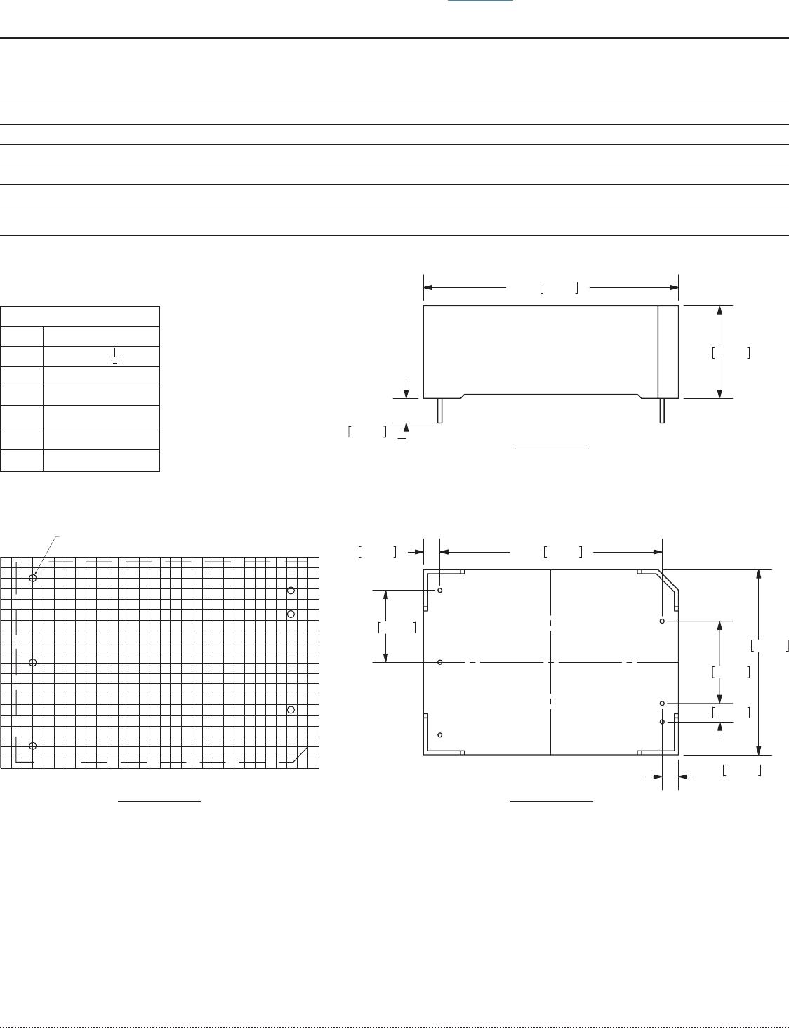
VSK-S20-5U

cui.com
date 06/11/2015 page 4 of 7CUI Inc SERIES: VSK-S20 DESCRIPTION: AC-DC POWER SUPPLY
BOTTOM VIEW
TOP VIEW
PCB LAYOUT
FRONT VIEW
6
2
3
1
5
4
4.00.157
0.78720.0
0.157
(2 PLCS)
0.90523.0
2.44162.0
4.0
48.01.889
(TYP)
70.0 2.756
6.0 0.236
23.5 0.925
2
1
3
Ø1.50[Ø0.059]
Grid size: 2.54 x 2.54
4
5
6
5.75 0.226
units: mm[inches]
tolerance: ±0.50[±0.020]
pin diameter: Ø1.00[0.039]±0.10[±0.004]
PIN CONNECTIONS
PIN FUNCTION
1 GND
2 AC(N)
3 AC(L)
4 TRIM
5 -Vo
6 +Vo
MECHANICAL
parameter conditions/description min typ max units
dimensions 70.0 x 48.0 x 23.5 (2.756 x 1.889 x 0.925 inch) mm
case material UL94V-0
weight 120 g
cooling convection cooling
MECHANICAL DRAWING
For more information, please visit the product page.
cui.com
date 06/11/2015 page 5 of 7CUI Inc SERIES: VSK-S20 DESCRIPTION: AC-DC POWER SUPPLY
AC(L)
+Vo
-Vo
AC(L)
AC(N)
AC(N)
C1 C2
TVS1
LO AD
FUSE
AC/DC
MOV1
TYPICAL APPLICATION CIRCUIT
Recommended External Circuit Components
MODEL FUSE MOV1 C1 C2 TVS
VSK-S20-3R3U
3.15A/250V S14K350 1µF 330μF SMBJ7.0A
VSK-S20-5U
3.15A/250V S14K350 1µF 330μF SMBJ7.0A
VSK-S20-9U
3.15A/250V S14K350 1µF 220μF SMBJ12A
VSK-S20-12U
3.15A/250V S14K350 1µF 220μF SMBJ20A
VSK-S20-15U
3.15A/250V S14K350 1µF 220μF SMBJ20A
VSK-S20-24U
3.15A/250V S14K350 1µF 220μF SMBJ30A
Recommended External Circuit Components
MOV1 S14K350
CY1, CY2 1000pF/400Vac
CX 0.1μF/275Vac
LCM 10mH
LDM 4.7μH/2A
EMC RECOMMENDED CIRCUIT
Note: Also refer to Table 1
Figure 1
Table 1
Figure 2
Table 2
ACDC
AC
(N)
AC(L)
LCM
MOV1
CX
CY1
CY2
FUSE
AC(N)
AC(L)
+Vo
-Vo
+
LDM
C1 C2 TVS1 RL
For more information, please visit the product page.
cui.com
date 06/11/2015 page 6 of 7CUI Inc SERIES: VSK-S20 DESCRIPTION: AC-DC POWER SUPPLY
APPLICATION NOTES
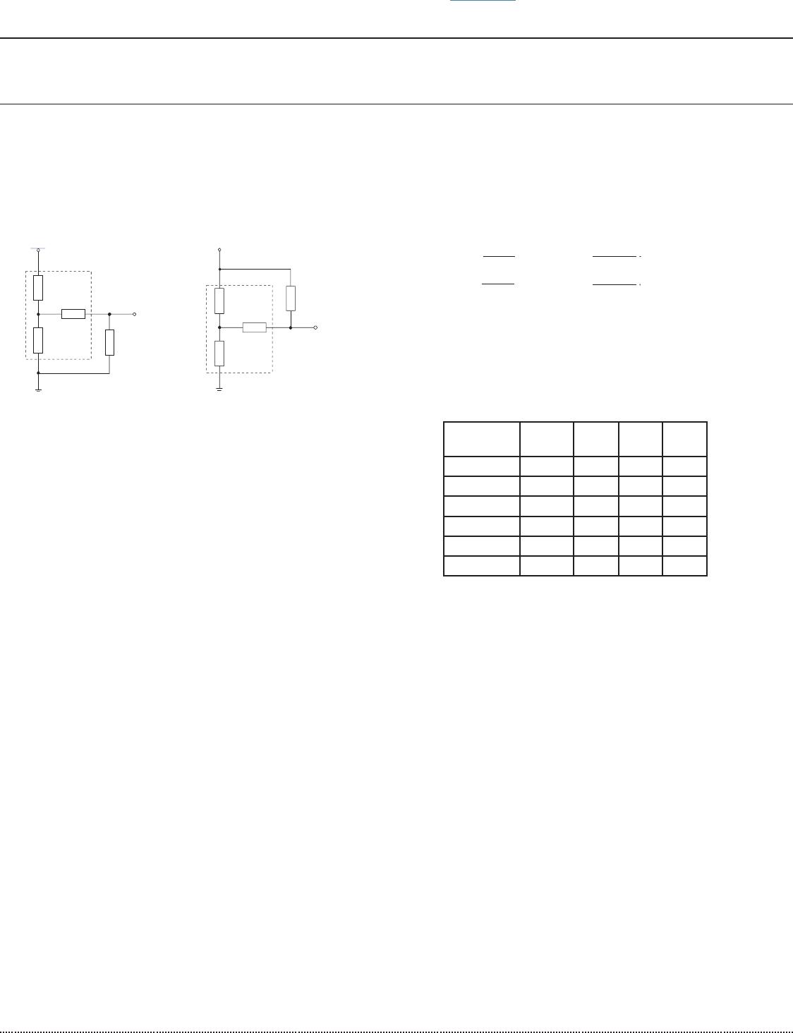
1. Output voltage trimming
Leave open if not used.
Application Circuit for Trim pin
(part in broken line is the interior of models) Formula for Trim Resistor
Note: Value for R1, R2, R3, and Vref refer to Table 3
R
T
: Trim Resistor
a: User-dened parameter, no actual meanings
Vo': The trim up/down voltage
Figure 3
Table 3
Vout
(Vdc)
R1
(kΩ)
R2
(kΩ)
R3
(kΩ)
Vref
(V)
3.3 3.3 1.98 1 1.24
5 3.3 3.3 1 2.5
9 7.5 2.87 1 2.5
12 3.83 1 1 2.5
15 7.5 1.5 1 2.5
24 8.66 1 1 2.5
+Vo
0V
R
2
R
1
R
3
V
re f
R
T
Trim
0V
R
2
R
1
R
3
V
ref
R
T
Tr
im
+Vo
Tr im up
Tr im down
a
-a
R
2
a
R 1
R2
-a
R1
-R3
-R3
: a=
Vref
Vref
Vo’ - Vref
Vo’ - Vref
R
1
R=
T
:
a=
R
2
R=
T
up
dow
n
Notes: 1. Output ltering capacitor C2 is an electrolytic capacitor, It is recommended to use high frequency and low impedance electrolytic capacitors. For capacitance and current
of capacitor please refer to manufacture’s datasheet. Voltage derating of capacitor should be 80% or above. C1 is used to lter high frequency noise. TVS is
recommended component to protect post-circuits (when converter fails).
2.
All specications measured at Ta=25C, humidity <75%, nominal input voltage, and rated output load, unless otherwise specied.
For more information, please visit the product page.

VSK-S20-5U

Mfr. #:
Manufacturer:
Description:
Switching Power Supplies ac-dc, 20 W, 5 Vdc, single output, encapsulated PCB
Lifecycle:
New from this manufacturer.
Delivery:
DHL FedEx Ups TNT EMS
Payment:
T/T Paypal Visa MoneyGram Western Union